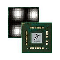
MPC8536DS Freescale Semiconductor, MPC8536DS Datasheet - Page 42

MPC8536DS
Manufacturer Part Number
MPC8536DS
Description
BOARD DEV SYSTEM MPC8536E
Manufacturer
Freescale Semiconductor
Series
PowerQUICC III™r
Type
MPUr
Datasheets
1.MPC8536EBVTAVLA.pdf
(127 pages)
2.MPC8536EBVTAVLA.pdf
(1706 pages)
3.MPC8536DS.pdf
(2 pages)
4.MPC8536DS.pdf
(126 pages)
Specifications of MPC8536DS
Contents
Board, Software and Documentation
Processor Series
MPC85xx
Core
e500
Data Bus Width
32 bit
Maximum Clock Frequency
667 MHz
Operating Supply Voltage
- 0.3 V to + 1.21 V
Maximum Operating Temperature
+ 105 C
Data Ram Size
32 KB
Interface Type
SPI, USB
Program Memory Type
DDR2, DDR3, SDRAM
Core Size
32 Bit
Program Memory Size
544KB
Cpu Speed
1.5GHz
Digital Ic Case Style
BGA
No. Of Pins
783
Supply Voltage Range
0.95V To 1.05V
Rohs Compliant
Yes
For Use With/related Products
MPC8536
Lead Free Status / RoHS Status
Lead free / RoHS Compliant
Ethernet: Enhanced Three-Speed Ethernet (eTSEC), MII Management
2.9.2
The AC timing specifications for FIFO, GMII, MII, TBI, RGMII, RMII, and RTBI are presented in this section.
2.9.2.1
The basis for the AC specifications for the eTSEC’s FIFO modes is the double data rate RGMII and RTBI specifications, since
they have similar performance and are described in a source-synchronous fashion like FIFO modes. However, the FIFO
interface provides deliberate skew between the transmitted data and source clock in GMII fashion.
When the eTSEC is configured for FIFO modes, all clocks are supplied from external sources to the relevant eTSEC interface.
That is, the transmit clock must be applied to the eTSECn’s TSECn_TX_CLK, while the receive clock must be applied to pin
TSECn_RX_CLK. The eTSEC internally uses the transmit clock to synchronously generate transmit data and outputs an echoed
copy of the transmit clock back out onto the TSECn_GTX_CLK pin (while transmit data appears on TSECn_TXD[7:0], for
example). It is intended that external receivers capture eTSEC transmit data using the clock on TSECn_GTX_CLK as a source-
synchronous timing reference. Typically, the clock edge that launched the data can be used, since the clock is delayed by the
eTSEC to allow acceptable set-up margin at the receiver. Note that there is relationship between the maximum FIFO speed and
the platform speed. For more information see
A summary of the FIFO AC specifications appears in
42
1
2
3
Supply voltage 2.5 V
Output high voltage
(LV
Output low voltage
(LV
Input high voltage
Input low voltage
Input high current
(V
Input low current
(V
Note:
TX_CLK, GTX_CLK clock period
TX_CLK, GTX_CLK duty cycle
TX_CLK, GTX_CLK peak-to-peak jitter
LV
TV
Note that the symbol V
IN
IN
DD
DD
= LV
= GND)
DD
DD
/TV
/TV
supports eTSECs 1.
supports eTSECs 3.
DD
DD
DD
, V
FIFO, GMII, MII, TBI, RGMII, RMII, and RTBI AC Timing Specifications
= Min, IOH = –1.0 mA)
= Min, I
FIFO AC Specifications
IN
Parameters
= TV
MPC8536E PowerQUICC III Integrated Processor Hardware Specifications, Rev. 3
Parameter/Condition
OL
DD
= 1.0 mA)
)
Table 25. RGMII, RTBI, and FIFO DC Electrical Characteristics
IN
, in this case, represents the LV
Table 26. FIFO Mode Transmit AC Timing Specification
2
Section 2.4.6, “Platform to FIFO Restrictions.”
LV
Symbol
DD
V
V
V
V
I
I
OH
/TV
OL
IH
IL
IH
IL
Table 26
DD
IN
GND – 0.3
and TV
and
Symbol
2.37
2.00
1.70
–0.3
Min
–15
—
t
t
t
FITH
FITJ
Table
FIT
IN
symbols referenced in
27.
LV
LV
Min
6.0
45
—
DD
DD
/TV
/TV
Max
2.63
0.40
0.70
10
—
DD
DD
+ 0.3
+ 0.3
Typ
8.0
50
—
Table 1
Freescale Semiconductor
Unit
μA
μA
Max
V
V
V
V
V
and
100
250
55
Table
2.
Notes
1, 2,3
Unit
1,2
ns
ps
%
—
—
—
—
3


