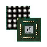
MPC8536DS Freescale Semiconductor, MPC8536DS Datasheet - Page 117

MPC8536DS
Manufacturer Part Number
MPC8536DS
Description
BOARD DEV SYSTEM MPC8536E
Manufacturer
Freescale Semiconductor
Series
PowerQUICC III™r
Type
MPUr
Datasheets
1.MPC8536EBVTAVLA.pdf
(127 pages)
2.MPC8536EBVTAVLA.pdf
(1706 pages)
3.MPC8536DS.pdf
(2 pages)
4.MPC8536DS.pdf
(126 pages)
Specifications of MPC8536DS
Contents
Board, Software and Documentation
Processor Series
MPC85xx
Core
e500
Data Bus Width
32 bit
Maximum Clock Frequency
667 MHz
Operating Supply Voltage
- 0.3 V to + 1.21 V
Maximum Operating Temperature
+ 105 C
Data Ram Size
32 KB
Interface Type
SPI, USB
Program Memory Type
DDR2, DDR3, SDRAM
Core Size
32 Bit
Program Memory Size
544KB
Cpu Speed
1.5GHz
Digital Ic Case Style
BGA
No. Of Pins
783
Supply Voltage Range
0.95V To 1.05V
Rohs Compliant
Yes
For Use With/related Products
MPC8536
Lead Free Status / RoHS Status
Lead free / RoHS Compliant
To measure Z
value of each resistor is varied until the pad voltage is OV
components, the resistances of the pull-up and pull-down devices. When data is held high, SW1 is closed (SW2 is open) and
R
are designed to be close to each other in value. Then, Z
Table 81
105°C.
Impedance
Note: Nominal supply voltages. See
3.9
The MPC8536E provides the user with power-on configuration options which can be set through the use of external pull-up or
pull-down resistors of 4.7 kΩ on certain output pins (see customer visible configuration pins). These pins are generally used as
output only pins in normal operation.
While HRESET is asserted however, these pins are treated as inputs. The value presented on these pins while HRESET is
asserted, is latched when HRESET deasserts, at which time the input receiver is disabled and the I/O circuit takes on its normal
function. Most of these sampled configuration pins are equipped with an on-chip gated resistor of approximately 20 kΩ. This
value should permit the 4.7-kΩ resistor to pull the configuration pin to a valid logic low level. The pull-up resistor is enabled
only during HRESET (and for platform /system clocks after HRESET deassertion to ensure capture of the reset value). When
the input receiver is disabled the pull-up is also, thus allowing functional operation of the pin as an output with minimal signal
quality or delay disruption. The default value for all configuration bits treated this way has been encoded such that a high voltage
Freescale Semiconductor
P
is trimmed until the voltage at the pad equals OV
R
R
N
P
summarizes the signal impedance targets. The driver impedances are targeted at minimum V
Configuration Pin Muxing
0
Control, Configuration, Power
Local Bus, Ethernet, DUART,
for the single-ended drivers, an external resistor is connected from the chip pad to OV
MPC8536E PowerQUICC III Integrated Processor Hardware Specifications, Rev. 3
Management
45 Target
45 Target
Table
Figure 77. Driver Impedance Measurement
Data
Table 81. Impedance Characteristics
1.
45 Target (cfg_pci_impd=1)
25 Target (cfg_pci_impd=0)
45 Target (cfg_pci_impd=1)
25 Target (cfg_pci_impd=0)
DD
0
/2. R
= (R
DD
P
/2 (see
P
PCI
then becomes the resistance of the pull-up devices. R
+ R
N
)/2.
Figure
Pad
R
R
OV
OGND
N
P
77). The output impedance is the average of two
DD
18 Target (full strength mode)
36 Target (full strength mode)
18 Target (full strength mode)
36 Target (full strength mode)
SW2
SW1
DDR DRAM
Configuration Pin Muxing
DD
DD
, nominal OV
or GND. Then, the
Symbol Unit
Z
Z
P
0
0
and R
DD
,
Ω
Ω
117
N


