DEMO9S08JM16 Freescale Semiconductor, DEMO9S08JM16 Datasheet - Page 201
DEMO9S08JM16
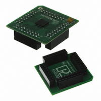
Manufacturer Part Number
DEMO9S08JM16
Description
BOARD DEMO FOR JM16 FAMI
Manufacturer
Freescale Semiconductor
Type
MCUr
Datasheets
1.DEMO9S08JM16.pdf
(47 pages)
2.DEMO9S08JM16.pdf
(5 pages)
3.DEMO9S08JM16.pdf
(4 pages)
4.DEMO9S08JM16.pdf
(386 pages)
Specifications of DEMO9S08JM16
Contents
Board with Daughter card, Cable, Documentation, Mini-AB USB Kit
Processor To Be Evaluated
MC9S08JM16
Data Bus Width
8 bit
Interface Type
USB
Silicon Manufacturer
Freescale
Core Architecture
HCS08
Core Sub-architecture
HCS08
Silicon Core Number
MC9S08
Silicon Family Name
Flexis - S08JM
Rohs Compliant
Yes
For Use With/related Products
MC9S08JM16
Lead Free Status / RoHS Status
Lead free / RoHS Compliant


12.5.2.3
In this example, the MCG will move through the proper operational modes from BLPI mode at a 16 kHz
bus frequency running off of the internal reference clock (see previous example) to FEE mode using a 4
MHz crystal configured for a 16 MHz bus frequency. First, the code sequence will be described. Then a
flowchart will be included which illustrates the sequence.
Freescale Semiconductor
1. First, BLPI must transition to FBI mode.
2. Next, FBI will transition to FEE mode.
a) MCGC2 = 0x00 (%00000000)
b) Optionally, loop until LOCK (bit 6) in the MCGSC is set, indicating that the FLL has acquired
a) MCGC2 = 0x36 (%00110110)
b) Loop until OSCINIT (bit 1) in MCGSC is 1, indicating the crystal selected by the EREFS bit
c) MCGC1 = 0x38 (%00111000)
d) Loop until IREFST (bit 4) in MCGSC is 0, indicating the external reference clock is the current
e) Optionally, loop until LOCK (bit 6) in the MCGSC is set, indicating that the FLL has
f) Loop until CLKST (bits 3 and 2) in MCGSC are %00, indicating that the output of the FLL is
– LP (bit 3) in MCGSC is 0
lock. Although the FLL is bypassed in FBI mode, it is still enabled and running.
– RANGE (bit 5) set to 1 because the frequency of 4 MHz is within the high frequency range
– HGO (bit 4) set to 1 to configure external oscillator for high gain operation
– EREFS (bit 2) set to 1, because a crystal is being used
– ERCLKEN (bit 1) set to 1 to ensure the external reference clock is active
has been initialized.
– CLKS (bits 7 and 6) set to %00 in order to select the output of the FLL as system clock
– RDIV (bits 5-3) set to %111, or divide-by-128 because 4 MHz / 128 = 31.25 kHz which is
– IREFS (bit 1) cleared to 0, selecting the external reference clock
source for the reference clock
reacquired lock.
selected to feed MCGOUT
Example #3: Moving from BLPI to FEE Mode: External Crystal = 4 MHz,
Bus Frequency = 16 MHz
source
in the 31.25 kHz to 39.0625 kHz range required by the FLL
MC9S08JM16 Series Data Sheet, Rev. 2
Multi-Purpose Clock Generator (S08MCGV1)
201
Related parts for DEMO9S08JM16
Image
Part Number
Description
Manufacturer
Datasheet
Request
R

Part Number:
Description:
Manufacturer:
Freescale Semiconductor, Inc
Datasheet:
Part Number:
Description:
Manufacturer:
Freescale Semiconductor, Inc
Datasheet:
Part Number:
Description:
Manufacturer:
Freescale Semiconductor, Inc
Datasheet:
Part Number:
Description:
Manufacturer:
Freescale Semiconductor, Inc
Datasheet:
Part Number:
Description:
Manufacturer:
Freescale Semiconductor, Inc
Datasheet:
Part Number:
Description:
Manufacturer:
Freescale Semiconductor, Inc
Datasheet:
Part Number:
Description:
Manufacturer:
Freescale Semiconductor, Inc
Datasheet:
Part Number:
Description:
Manufacturer:
Freescale Semiconductor, Inc
Datasheet:
Part Number:
Description:
Manufacturer:
Freescale Semiconductor, Inc
Datasheet:
Part Number:
Description:
Manufacturer:
Freescale Semiconductor, Inc
Datasheet:
Part Number:
Description:
Manufacturer:
Freescale Semiconductor, Inc
Datasheet:
Part Number:
Description:
Manufacturer:
Freescale Semiconductor, Inc
Datasheet:
Part Number:
Description:
Manufacturer:
Freescale Semiconductor, Inc
Datasheet:
Part Number:
Description:
Manufacturer:
Freescale Semiconductor, Inc
Datasheet:
Part Number:
Description:
Manufacturer:
Freescale Semiconductor, Inc
Datasheet: