DEMO9S08JM16 Freescale Semiconductor, DEMO9S08JM16 Datasheet - Page 354
DEMO9S08JM16
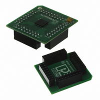
Manufacturer Part Number
DEMO9S08JM16
Description
BOARD DEMO FOR JM16 FAMI
Manufacturer
Freescale Semiconductor
Type
MCUr
Datasheets
1.DEMO9S08JM16.pdf
(47 pages)
2.DEMO9S08JM16.pdf
(5 pages)
3.DEMO9S08JM16.pdf
(4 pages)
4.DEMO9S08JM16.pdf
(386 pages)
Specifications of DEMO9S08JM16
Contents
Board with Daughter card, Cable, Documentation, Mini-AB USB Kit
Processor To Be Evaluated
MC9S08JM16
Data Bus Width
8 bit
Interface Type
USB
Silicon Manufacturer
Freescale
Core Architecture
HCS08
Core Sub-architecture
HCS08
Silicon Core Number
MC9S08
Silicon Family Name
Flexis - S08JM
Rohs Compliant
Yes
For Use With/related Products
MC9S08JM16
Lead Free Status / RoHS Status
Lead free / RoHS Compliant


Appendix A Electrical Characteristics
354
3
4
5
6
7
8
Measured with V
Measured with V
Power supply must maintain regulation within operating V
current conditions. If positive injection current (V
V
greater than maximum injection current. This will be the greatest risk when the MCU is not consuming power.
Examples are: if no system clock is present, or if clock rate is very low (which would reduce overall power
consumption).
All functional non-supply pins are internally clamped to V
Input must be current limited to the value specified. To determine the value of the required current-limiting resistor,
calculate resistance values for positive and negative clamp voltages, then use the larger of the two values.
The RESET pin does not have a clamp diode to V
DD
and could result in external power supply going out of regulation. Ensure external V
0.5
0.4
0.4
0.3
0.3
0.2
0.2
0.1
0.1
0.0
Figure A-1. Typical Low-Side Drive (Sink) Characteristics – High Drive (PTxDSn = 1)
Figure A-2. Typical Low-Side Drive (Sink) Characteristics – Low Drive (PTxDSn = 0)
0.7
0.6
0.5
0.4
0.3
0.2
0.1
0.0
0
1
0
Typical V
Hot (85°C)
Room (25°C )
Cold (-40°C)
2
T ypical V
In
In
Hot (85°C)
Room (25°C)
Cold (-40°C)
3
= V
= V
4
OL
5
SS
DD
O L
1
vs. I
6
v s. I
.
.
I
OL
I
OL
7
(m A)
O L
(mA)
OL
8
AT V
AT V
9
2
D D
10
MC9S08JM16 Series Data Sheet, Rev. 2
DD
= 5V
11
= 5V
12
13
3
14
15
In
DD
> V
. Do not drive this pin above V
DD
) is greater than I
SS
DD
and V
range during instantaneous and operating maximum
0 .8
0 .7
0 .6
0 .5
0 .4
0 .3
0 .2
0 .1
0 .0
1.400
1.200
1.000
0.800
0.600
0.400
0.200
0.000
0.0
DD
.
1
Typical V
0
T y p ic a l V
2
H o t (8 5 ° C )
R o o m (2 5 ° C )
C o ld (-4 0 ° C )
3
DD
Hot (85°C)
Room (25°C)
Cold (-40°C)
4
, the injection current may flow out of
OL
O L
5
1
I
v s . I
OL
vs. I
6
I
O L
(mA)
7
DD
O L
(m A )
OL
8
A T V
.
AT V
9
DD
2
10
DD
load will shunt current
DD
= 3 V
11
Freescale Semiconductor
= 3V
12
13
3
14
15
Related parts for DEMO9S08JM16
Image
Part Number
Description
Manufacturer
Datasheet
Request
R

Part Number:
Description:
Manufacturer:
Freescale Semiconductor, Inc
Datasheet:
Part Number:
Description:
Manufacturer:
Freescale Semiconductor, Inc
Datasheet:
Part Number:
Description:
Manufacturer:
Freescale Semiconductor, Inc
Datasheet:
Part Number:
Description:
Manufacturer:
Freescale Semiconductor, Inc
Datasheet:
Part Number:
Description:
Manufacturer:
Freescale Semiconductor, Inc
Datasheet:
Part Number:
Description:
Manufacturer:
Freescale Semiconductor, Inc
Datasheet:
Part Number:
Description:
Manufacturer:
Freescale Semiconductor, Inc
Datasheet:
Part Number:
Description:
Manufacturer:
Freescale Semiconductor, Inc
Datasheet:
Part Number:
Description:
Manufacturer:
Freescale Semiconductor, Inc
Datasheet:
Part Number:
Description:
Manufacturer:
Freescale Semiconductor, Inc
Datasheet:
Part Number:
Description:
Manufacturer:
Freescale Semiconductor, Inc
Datasheet:
Part Number:
Description:
Manufacturer:
Freescale Semiconductor, Inc
Datasheet:
Part Number:
Description:
Manufacturer:
Freescale Semiconductor, Inc
Datasheet:
Part Number:
Description:
Manufacturer:
Freescale Semiconductor, Inc
Datasheet:
Part Number:
Description:
Manufacturer:
Freescale Semiconductor, Inc
Datasheet: