DEMO9S08JM16 Freescale Semiconductor, DEMO9S08JM16 Datasheet - Page 78
DEMO9S08JM16
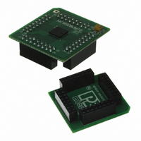
Manufacturer Part Number
DEMO9S08JM16
Description
BOARD DEMO FOR JM16 FAMI
Manufacturer
Freescale Semiconductor
Type
MCUr
Datasheets
1.DEMO9S08JM16.pdf
(47 pages)
2.DEMO9S08JM16.pdf
(5 pages)
3.DEMO9S08JM16.pdf
(4 pages)
4.DEMO9S08JM16.pdf
(386 pages)
Specifications of DEMO9S08JM16
Contents
Board with Daughter card, Cable, Documentation, Mini-AB USB Kit
Processor To Be Evaluated
MC9S08JM16
Data Bus Width
8 bit
Interface Type
USB
Silicon Manufacturer
Freescale
Core Architecture
HCS08
Core Sub-architecture
HCS08
Silicon Core Number
MC9S08
Silicon Family Name
Flexis - S08JM
Rohs Compliant
Yes
For Use With/related Products
MC9S08JM16
Lead Free Status / RoHS Status
Lead free / RoHS Compliant


Chapter 6 Parallel Input/Output
6.2
Reading and writing of parallel I/O is done through the port data registers. The direction, input or output,
is controlled through the port data direction registers. The parallel I/O port function for an individual pin
is illustrated in the block diagram below.
The data direction control bits determine whether the pin output driver is enabled, and they control what
is read for port data register reads. Each port pin has a data direction register bit. When PTxDDn = 0, the
corresponding pin is an input and reads of PTxD return the pin value. When PTxDDn = 1, the
corresponding pin is an output and reads of PTxD return the last value written to the port data register.
When a peripheral module or system function is in control of a port pin, the data direction register bit still
controls what is returned for reads of the port data register, even though the peripheral system has
overriding control of the actual pin direction.
When a shared analog function is enabled for a pin, all digital pin functions are disabled. A read of the port
data register returns a value of 0 for any bits which have shared analog functions enabled. In general,
whenever a pin is shared with both an alternate digital function and an analog function, the analog function
has priority such that if both the digital and analog functions are enabled, the analog function controls the
pin.
Write to the port data register before changing the direction of a port pin to become an output. This ensures
that the pin will not be driven momentarily with an old data value that happened to be in the port data
register.
78
Port Data and Data Direction
Port Read
BUSCLK
Data
PTxDDn
D
D
PTxDn
Figure 6-1. Parallel I/O Block Diagram
MC9S08JM16 Series Data Sheet, Rev. 2
Q
Q
1
0
Synchronizer
Output Enable
Output Data
Freescale Semiconductor
Input Data
Related parts for DEMO9S08JM16
Image
Part Number
Description
Manufacturer
Datasheet
Request
R

Part Number:
Description:
Manufacturer:
Freescale Semiconductor, Inc
Datasheet:
Part Number:
Description:
Manufacturer:
Freescale Semiconductor, Inc
Datasheet:
Part Number:
Description:
Manufacturer:
Freescale Semiconductor, Inc
Datasheet:
Part Number:
Description:
Manufacturer:
Freescale Semiconductor, Inc
Datasheet:
Part Number:
Description:
Manufacturer:
Freescale Semiconductor, Inc
Datasheet:
Part Number:
Description:
Manufacturer:
Freescale Semiconductor, Inc
Datasheet:
Part Number:
Description:
Manufacturer:
Freescale Semiconductor, Inc
Datasheet:
Part Number:
Description:
Manufacturer:
Freescale Semiconductor, Inc
Datasheet:
Part Number:
Description:
Manufacturer:
Freescale Semiconductor, Inc
Datasheet:
Part Number:
Description:
Manufacturer:
Freescale Semiconductor, Inc
Datasheet:
Part Number:
Description:
Manufacturer:
Freescale Semiconductor, Inc
Datasheet:
Part Number:
Description:
Manufacturer:
Freescale Semiconductor, Inc
Datasheet:
Part Number:
Description:
Manufacturer:
Freescale Semiconductor, Inc
Datasheet:
Part Number:
Description:
Manufacturer:
Freescale Semiconductor, Inc
Datasheet:
Part Number:
Description:
Manufacturer:
Freescale Semiconductor, Inc
Datasheet: