DEMO9S08JM16 Freescale Semiconductor, DEMO9S08JM16 Datasheet - Page 243
DEMO9S08JM16
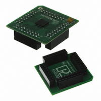
Manufacturer Part Number
DEMO9S08JM16
Description
BOARD DEMO FOR JM16 FAMI
Manufacturer
Freescale Semiconductor
Type
MCUr
Datasheets
1.DEMO9S08JM16.pdf
(47 pages)
2.DEMO9S08JM16.pdf
(5 pages)
3.DEMO9S08JM16.pdf
(4 pages)
4.DEMO9S08JM16.pdf
(386 pages)
Specifications of DEMO9S08JM16
Contents
Board with Daughter card, Cable, Documentation, Mini-AB USB Kit
Processor To Be Evaluated
MC9S08JM16
Data Bus Width
8 bit
Interface Type
USB
Silicon Manufacturer
Freescale
Core Architecture
HCS08
Core Sub-architecture
HCS08
Silicon Core Number
MC9S08
Silicon Family Name
Flexis - S08JM
Rohs Compliant
Yes
For Use With/related Products
MC9S08JM16
Lead Free Status / RoHS Status
Lead free / RoHS Compliant


15.1.4.1
Figure 15-3
device initiates all SPI data transfers. During a transfer, the master shifts data out (on the MOSI pin) to the
slave while simultaneously shifting data in (on the MISO pin) from the slave. The transfer effectively
exchanges the data that was in the SPI shift registers of the two SPI systems. The SPSCK signal is a clock
output from the master and an input to the slave. The slave device must be selected by a low level on the
slave select input (SS pin). In this system, the master device has configured its SS pin as an optional slave
select output.
15.1.4.2
Figure 15-4
Data is written to the double-buffered transmitter (write to SPIxDH:SPIxDL) and gets transferred to the
SPI shift register at the start of a data transfer. After shifting in 8 or 16 bits (as determined by SPIMODE
bit) of data, the data is transferred into the double-buffered receiver where it can be read (read from
SPIxDH:SPIxDL). Pin multiplexing logic controls connections between MCU pins and the SPI module.
When the SPI is configured as a master, the clock output is routed to the SPSCK pin, the shifter output is
routed to MOSI, and the shifter input is routed from the MISO pin.
When the SPI is configured as a slave, the SPSCK pin is routed to the clock input of the SPI, the shifter
output is routed to MISO, and the shifter input is routed from the MOSI pin.
In the external SPI system, simply connect all SPSCK pins to each other, all MISO pins together, and all
MOSI pins together. Peripheral devices often use slightly different names for these pins.
Freescale Semiconductor
is a block diagram of the SPI module. The central element of the SPI is the SPI shift register.
shows the SPI modules of two MCUs connected in a master-slave arrangement. The master
SPI System Block Diagram
SPI Module Block Diagram
GENERATOR
SPI SHIFTER
8 OR 16 BITS
MASTER
CLOCK
Figure 15-3. SPI System Connections
MC9S08JM16 Series Data Sheet, Rev. 2
MOSI
MISO
SPSCK
SS
SPSCK
MOSI
MISO
SS
SLAVE
Serial Peripheral Interface (S08SPI16V1)
SPI SHIFTER
8 OR 16 BITS
243
Related parts for DEMO9S08JM16
Image
Part Number
Description
Manufacturer
Datasheet
Request
R

Part Number:
Description:
Manufacturer:
Freescale Semiconductor, Inc
Datasheet:
Part Number:
Description:
Manufacturer:
Freescale Semiconductor, Inc
Datasheet:
Part Number:
Description:
Manufacturer:
Freescale Semiconductor, Inc
Datasheet:
Part Number:
Description:
Manufacturer:
Freescale Semiconductor, Inc
Datasheet:
Part Number:
Description:
Manufacturer:
Freescale Semiconductor, Inc
Datasheet:
Part Number:
Description:
Manufacturer:
Freescale Semiconductor, Inc
Datasheet:
Part Number:
Description:
Manufacturer:
Freescale Semiconductor, Inc
Datasheet:
Part Number:
Description:
Manufacturer:
Freescale Semiconductor, Inc
Datasheet:
Part Number:
Description:
Manufacturer:
Freescale Semiconductor, Inc
Datasheet:
Part Number:
Description:
Manufacturer:
Freescale Semiconductor, Inc
Datasheet:
Part Number:
Description:
Manufacturer:
Freescale Semiconductor, Inc
Datasheet:
Part Number:
Description:
Manufacturer:
Freescale Semiconductor, Inc
Datasheet:
Part Number:
Description:
Manufacturer:
Freescale Semiconductor, Inc
Datasheet:
Part Number:
Description:
Manufacturer:
Freescale Semiconductor, Inc
Datasheet:
Part Number:
Description:
Manufacturer:
Freescale Semiconductor, Inc
Datasheet: