DEMO9S08JM16 Freescale Semiconductor, DEMO9S08JM16 Datasheet - Page 255
DEMO9S08JM16
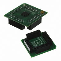
Manufacturer Part Number
DEMO9S08JM16
Description
BOARD DEMO FOR JM16 FAMI
Manufacturer
Freescale Semiconductor
Type
MCUr
Datasheets
1.DEMO9S08JM16.pdf
(47 pages)
2.DEMO9S08JM16.pdf
(5 pages)
3.DEMO9S08JM16.pdf
(4 pages)
4.DEMO9S08JM16.pdf
(386 pages)
Specifications of DEMO9S08JM16
Contents
Board with Daughter card, Cable, Documentation, Mini-AB USB Kit
Processor To Be Evaluated
MC9S08JM16
Data Bus Width
8 bit
Interface Type
USB
Silicon Manufacturer
Freescale
Core Architecture
HCS08
Core Sub-architecture
HCS08
Silicon Core Number
MC9S08
Silicon Family Name
Flexis - S08JM
Rohs Compliant
Yes
For Use With/related Products
MC9S08JM16
Lead Free Status / RoHS Status
Lead free / RoHS Compliant


Any switching between 8- and 16-bit data transmission length (controlled by SPIMODE bit) in master
mode will abort a transmission in progress, force the SPI system into idle state, and reset all status bits in
the SPIxS register. To initiate a transfer after writing to SPIMODE, the SPIxS register must be read with
SPTEF = 1, and data must be written to SPIxDH:SPIxDL in 16-bit mode (SPIMODE = 1) or SPIxDL in
8-bit mode (SPIMODE = 0).
In slave mode, user software must write to SPIMODE only once to prevent corrupting a transmission in
progress.
15.4.5
To accommodate a wide variety of synchronous serial peripherals from different manufacturers, the SPI
system has a clock polarity (CPOL) bit and a clock phase (CPHA) control bit to select one of four clock
formats for data transfers. CPOL selectively inserts an inverter in series with the clock. CPHA chooses
between two different clock phase relationships between the clock and data.
Figure 15-13
figure, the eight bit times are shown for reference with bit 1 starting at the first SPSCK edge and bit 8
ending one-half SPSCK cycle after the sixteenth SPSCK edge. The MSB first and LSB first lines show the
order of SPI data bits depending on the setting in LSBFE. Both variations of SPSCK polarity are shown,
but only one of these waveforms applies for a specific transfer, depending on the value in CPOL. The
SAMPLE IN waveform applies to the MOSI input of a slave or the MISO input of a master. The MOSI
waveform applies to the MOSI output pin from a master and the MISO waveform applies to the MISO
output from a slave. The SS OUT waveform applies to the slave select output from a master (provided
MODFEN and SSOE = 1). The master SS output goes to active low one-half SPSCK cycle before the start
of the transfer and goes back high at the end of the eighth bit time of the transfer. The SS IN waveform
applies to the slave select input of a slave.
Freescale Semiconductor
SPI Clock Formats
shows the clock formats when SPIMODE = 0 (8-bit mode) and CPHA = 1. At the top of the
Data can be lost if the data length is not the same for both master and slave
devices.
MC9S08JM16 Series Data Sheet, Rev. 2
NOTE
Serial Peripheral Interface (S08SPI16V1)
255
Related parts for DEMO9S08JM16
Image
Part Number
Description
Manufacturer
Datasheet
Request
R

Part Number:
Description:
Manufacturer:
Freescale Semiconductor, Inc
Datasheet:
Part Number:
Description:
Manufacturer:
Freescale Semiconductor, Inc
Datasheet:
Part Number:
Description:
Manufacturer:
Freescale Semiconductor, Inc
Datasheet:
Part Number:
Description:
Manufacturer:
Freescale Semiconductor, Inc
Datasheet:
Part Number:
Description:
Manufacturer:
Freescale Semiconductor, Inc
Datasheet:
Part Number:
Description:
Manufacturer:
Freescale Semiconductor, Inc
Datasheet:
Part Number:
Description:
Manufacturer:
Freescale Semiconductor, Inc
Datasheet:
Part Number:
Description:
Manufacturer:
Freescale Semiconductor, Inc
Datasheet:
Part Number:
Description:
Manufacturer:
Freescale Semiconductor, Inc
Datasheet:
Part Number:
Description:
Manufacturer:
Freescale Semiconductor, Inc
Datasheet:
Part Number:
Description:
Manufacturer:
Freescale Semiconductor, Inc
Datasheet:
Part Number:
Description:
Manufacturer:
Freescale Semiconductor, Inc
Datasheet:
Part Number:
Description:
Manufacturer:
Freescale Semiconductor, Inc
Datasheet:
Part Number:
Description:
Manufacturer:
Freescale Semiconductor, Inc
Datasheet:
Part Number:
Description:
Manufacturer:
Freescale Semiconductor, Inc
Datasheet: