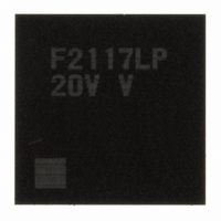
DF2117VLP20V Renesas Electronics America, DF2117VLP20V Datasheet - Page 25

DF2117VLP20V
Manufacturer Part Number
DF2117VLP20V
Description
IC H8S/2117 MCU FLASH 145TFLGA
Manufacturer
Renesas Electronics America
Series
H8® H8S/2100r
Datasheet
1.DF2117VBG20V.pdf
(960 pages)
Specifications of DF2117VLP20V
Core Processor
H8S/2600
Core Size
16-Bit
Speed
20MHz
Connectivity
FIFO, I²C, LPC, SCI, SmartCard
Peripherals
POR, PWM, WDT
Number Of I /o
112
Program Memory Size
160KB (160K x 8)
Program Memory Type
FLASH
Ram Size
8K x 8
Voltage - Supply (vcc/vdd)
3 V ~ 3.6 V
Data Converters
A/D 16x10b
Oscillator Type
External
Operating Temperature
-20°C ~ 75°C
Package / Case
145-TFLGA
For Use With
HS0005KCU11H - EMULATOR E10A-USB H8S(X),SH2(A)3DK2166 - DEV EVAL KIT H8S/2166
Lead Free Status / RoHS Status
Lead free / RoHS Compliant
Eeprom Size
-
Available stocks
Company
Part Number
Manufacturer
Quantity
Price
Company:
Part Number:
DF2117VLP20V
Manufacturer:
Renesas
Quantity:
100
Part Number:
DF2117VLP20V
Manufacturer:
RENESAS/瑞萨
Quantity:
20 000
- Current page: 25 of 960
- Download datasheet (6Mb)
Item
22.12 Standard Serial
Communication Interface
Specifications for Boot Mode
Figure 22.18 Boot Program
States
Table 22.17 Inquiry and
Selection Commands
(3) Inquiry and Selection States
(f) Operating Clock Frequency
Inquiry
(8) Programming/Erasing State
(c) 128-Byte Programming
Page Revision (See Manual for Details)
729
732
737
750
Figure amended
Table amended
Description amended
• Minimum value of operating clock frequency (two
• Maximum value (two bytes): Maximum value among
Description amended
• ERROR: (one byte): Error code
Command
H'40
bytes): The minimum value of the
frequency.
The minimum and maximum values of the operating
clock frequency represent the values in MHz, valid
to the hundredths place of MHz, and multiplied by
100. (e.g. when the value is 20.00 MHz, it will be
2000, which is H'07D0.)
the
There are as many pairs of minimum and maximum
values as there are operating clock frequencies.
H'11: Checksum Error
H'2A: Address error
H'53: Programming error
Operations for erasing
Programming/
erasing wait
user MATs and
user boot MATs
Command Name
Transition to
programming/erasing state
Programming
divided clock frequencies.
The address is not within the specified MAT
range.
A programming error has occurred and
programming cannot be continued.
Operations for
programming
Rev. 3.00 Sep. 28, 2009 Page xxiii of xliv
Description
Erasing of user MATs or user boot MATs, and entry
to programming/erasing state
Erasing
Operations for
erasing
REJ09B0350-0300
divided clock
Checking
Operations for
checking
Related parts for DF2117VLP20V
Image
Part Number
Description
Manufacturer
Datasheet
Request
R

Part Number:
Description:
KIT STARTER FOR M16C/29
Manufacturer:
Renesas Electronics America
Datasheet:

Part Number:
Description:
KIT STARTER FOR R8C/2D
Manufacturer:
Renesas Electronics America
Datasheet:

Part Number:
Description:
R0K33062P STARTER KIT
Manufacturer:
Renesas Electronics America
Datasheet:

Part Number:
Description:
KIT STARTER FOR R8C/23 E8A
Manufacturer:
Renesas Electronics America
Datasheet:

Part Number:
Description:
KIT STARTER FOR R8C/25
Manufacturer:
Renesas Electronics America
Datasheet:

Part Number:
Description:
KIT STARTER H8S2456 SHARPE DSPLY
Manufacturer:
Renesas Electronics America
Datasheet:

Part Number:
Description:
KIT STARTER FOR R8C38C
Manufacturer:
Renesas Electronics America
Datasheet:

Part Number:
Description:
KIT STARTER FOR R8C35C
Manufacturer:
Renesas Electronics America
Datasheet:

Part Number:
Description:
KIT STARTER FOR R8CL3AC+LCD APPS
Manufacturer:
Renesas Electronics America
Datasheet:

Part Number:
Description:
KIT STARTER FOR RX610
Manufacturer:
Renesas Electronics America
Datasheet:

Part Number:
Description:
KIT STARTER FOR R32C/118
Manufacturer:
Renesas Electronics America
Datasheet:

Part Number:
Description:
KIT DEV RSK-R8C/26-29
Manufacturer:
Renesas Electronics America
Datasheet:

Part Number:
Description:
KIT STARTER FOR SH7124
Manufacturer:
Renesas Electronics America
Datasheet:

Part Number:
Description:
KIT STARTER FOR H8SX/1622
Manufacturer:
Renesas Electronics America
Datasheet:

Part Number:
Description:
KIT DEV FOR SH7203
Manufacturer:
Renesas Electronics America
Datasheet:


