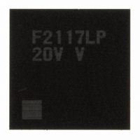
DF2117VLP20V Renesas Electronics America, DF2117VLP20V Datasheet - Page 757

DF2117VLP20V
Manufacturer Part Number
DF2117VLP20V
Description
IC H8S/2117 MCU FLASH 145TFLGA
Manufacturer
Renesas Electronics America
Series
H8® H8S/2100r
Datasheet
1.DF2117VBG20V.pdf
(960 pages)
Specifications of DF2117VLP20V
Core Processor
H8S/2600
Core Size
16-Bit
Speed
20MHz
Connectivity
FIFO, I²C, LPC, SCI, SmartCard
Peripherals
POR, PWM, WDT
Number Of I /o
112
Program Memory Size
160KB (160K x 8)
Program Memory Type
FLASH
Ram Size
8K x 8
Voltage - Supply (vcc/vdd)
3 V ~ 3.6 V
Data Converters
A/D 16x10b
Oscillator Type
External
Operating Temperature
-20°C ~ 75°C
Package / Case
145-TFLGA
For Use With
HS0005KCU11H - EMULATOR E10A-USB H8S(X),SH2(A)3DK2166 - DEV EVAL KIT H8S/2166
Lead Free Status / RoHS Status
Lead free / RoHS Compliant
Eeprom Size
-
Available stocks
Company
Part Number
Manufacturer
Quantity
Price
Company:
Part Number:
DF2117VLP20V
Manufacturer:
Renesas
Quantity:
100
Part Number:
DF2117VLP20V
Manufacturer:
RENESAS/瑞萨
Quantity:
20 000
- Current page: 757 of 960
- Download datasheet (6Mb)
8. All interrupts and the use of a bus master other than the CPU are disabled during
9. FKEY must be set to H'5A and the user MAT must be prepared for programming.
10. The parameters required for programming are set. The start address of the programming
11. Programming is executed. The entry point of the programming program is at the address which
12. The return value in the programming program, the FPFR parameter is determined.
13. Determine whether programming of the necessary data has finished. If more than 128 bytes of
MOV.L
JSR
NOP
programming/erasing. The specified voltage is applied for the specified time when
programming or erasing. If interrupts occur or the bus mastership is moved to other than the
CPU during programming/erasing, causing a voltage exceeding the specifications to be
applied, the flash memory may be damaged. Therefore, interrupts are disabled by setting bit 7
(I bit) in the condition code register (CCR) to B'1 in interrupt control mode 0 and by setting
bits 2 to 0 (I2 to I0 bits) in the extend register (EXR) to B'111 in interrupt control mode 2.
Accordingly, interrupts other than NMI are held and not executed. Configure the user system
so that NMI interrupts do not occur. The interrupts that are held must be executed after all
programming completes.
destination on the user MAT (FMPAR parameter) is set in general register ER1. The start
address of the program data storage area (FMPDR parameter) is set in general register ER0.
⎯ Example of FMPAR parameter setting: When an address other than one in the user MAT
⎯ Example of FMPDR parameter setting: When the storage destination for the program data
is 16 bytes after #DLTOP (start address of the download destination specified by FTDAR).
Call the subroutine to execute programming by using the following steps.
⎯ The general registers other than R0L are held in the programming program.
⎯ R0L is a return value of the FPFR parameter.
⎯ Since the stack area is used in the programming program, a stack area of 128 bytes at the
data are to be programmed, update the FMPAR and FMPDR parameters in 128-byte units, and
repeat steps 11 to 14. Increment the programming destination address by 128 bytes and update
the programming data pointer correctly. If an address which has already been programmed is
written to again, not only will a programming error occur, but also flash memory will be
damaged.
area is specified for the start address of the programming destination, even if the
programming program is executed, programming is not executed and an error is returned to
the FPFR parameter. Since the program data for one programming operation is 128 bytes,
the lower eight bits of the address must be H'00 or H'80 to be aligned with the 128-byte
boundary.
is flash memory, even if the programming routine is executed, programming is not
executed and an error is returned to the FPFR parameter. In this case, the program data
must be transferred to the on-chip RAM and then programming must be executed.
maximum must be allocated in RAM.
#DLTOP+16,ER2
@ER2
; Set entry address to ER2
; Call programming routine
Rev. 3.00 Sep. 28, 2009 Page 711 of 910
Section 22 Flash Memory
REJ09B0350-0300
Related parts for DF2117VLP20V
Image
Part Number
Description
Manufacturer
Datasheet
Request
R

Part Number:
Description:
KIT STARTER FOR M16C/29
Manufacturer:
Renesas Electronics America
Datasheet:

Part Number:
Description:
KIT STARTER FOR R8C/2D
Manufacturer:
Renesas Electronics America
Datasheet:

Part Number:
Description:
R0K33062P STARTER KIT
Manufacturer:
Renesas Electronics America
Datasheet:

Part Number:
Description:
KIT STARTER FOR R8C/23 E8A
Manufacturer:
Renesas Electronics America
Datasheet:

Part Number:
Description:
KIT STARTER FOR R8C/25
Manufacturer:
Renesas Electronics America
Datasheet:

Part Number:
Description:
KIT STARTER H8S2456 SHARPE DSPLY
Manufacturer:
Renesas Electronics America
Datasheet:

Part Number:
Description:
KIT STARTER FOR R8C38C
Manufacturer:
Renesas Electronics America
Datasheet:

Part Number:
Description:
KIT STARTER FOR R8C35C
Manufacturer:
Renesas Electronics America
Datasheet:

Part Number:
Description:
KIT STARTER FOR R8CL3AC+LCD APPS
Manufacturer:
Renesas Electronics America
Datasheet:

Part Number:
Description:
KIT STARTER FOR RX610
Manufacturer:
Renesas Electronics America
Datasheet:

Part Number:
Description:
KIT STARTER FOR R32C/118
Manufacturer:
Renesas Electronics America
Datasheet:

Part Number:
Description:
KIT DEV RSK-R8C/26-29
Manufacturer:
Renesas Electronics America
Datasheet:

Part Number:
Description:
KIT STARTER FOR SH7124
Manufacturer:
Renesas Electronics America
Datasheet:

Part Number:
Description:
KIT STARTER FOR H8SX/1622
Manufacturer:
Renesas Electronics America
Datasheet:

Part Number:
Description:
KIT DEV FOR SH7203
Manufacturer:
Renesas Electronics America
Datasheet:


