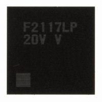
DF2117VLP20V Renesas Electronics America, DF2117VLP20V Datasheet - Page 557

DF2117VLP20V
Manufacturer Part Number
DF2117VLP20V
Description
IC H8S/2117 MCU FLASH 145TFLGA
Manufacturer
Renesas Electronics America
Series
H8® H8S/2100r
Datasheet
1.DF2117VBG20V.pdf
(960 pages)
Specifications of DF2117VLP20V
Core Processor
H8S/2600
Core Size
16-Bit
Speed
20MHz
Connectivity
FIFO, I²C, LPC, SCI, SmartCard
Peripherals
POR, PWM, WDT
Number Of I /o
112
Program Memory Size
160KB (160K x 8)
Program Memory Type
FLASH
Ram Size
8K x 8
Voltage - Supply (vcc/vdd)
3 V ~ 3.6 V
Data Converters
A/D 16x10b
Oscillator Type
External
Operating Temperature
-20°C ~ 75°C
Package / Case
145-TFLGA
For Use With
HS0005KCU11H - EMULATOR E10A-USB H8S(X),SH2(A)3DK2166 - DEV EVAL KIT H8S/2166
Lead Free Status / RoHS Status
Lead free / RoHS Compliant
Eeprom Size
-
Available stocks
Company
Part Number
Manufacturer
Quantity
Price
Company:
Part Number:
DF2117VLP20V
Manufacturer:
Renesas
Quantity:
100
Part Number:
DF2117VLP20V
Manufacturer:
RENESAS/瑞萨
Quantity:
20 000
- Current page: 557 of 960
- Download datasheet (6Mb)
17.3.3
SARX sets the second slave address and selects the communication format. If the LSI is in slave
mode with the I
match the upper 7 bits of the first frame received after a start condition, the LSI operates as the
slave device specified by the master device. SARX can be accessed only when the ICE bit in
ICCR is cleared to 0.
Bit
7
6
5
4
3
2
1
0
Bit Name
SVAX6
SVAX5
SVAX4
SVAX3
SVAX2
SVAX1
SVAX0
FSX
Second Slave Address Register (SARX)
2
C bus format selected, when the FSX bit is set to 0 and the upper 7 bits of SARX
Initial
Value
0
0
0
0
0
0
0
1
R/W
R/W
R/W
R/W
R/W
R/W
R/W
R/W
R/W
Description
Second Slave Address 6 to 0
Set the second slave address.
Format Select X
Selects the communication format together with the FS
bit in SAR. See table 17.3.
Rev. 3.00 Sep. 28, 2009 Page 511 of 910
Section 17 I
2
C Bus Interface (IIC)
REJ09B0350-0300
Related parts for DF2117VLP20V
Image
Part Number
Description
Manufacturer
Datasheet
Request
R

Part Number:
Description:
KIT STARTER FOR M16C/29
Manufacturer:
Renesas Electronics America
Datasheet:

Part Number:
Description:
KIT STARTER FOR R8C/2D
Manufacturer:
Renesas Electronics America
Datasheet:

Part Number:
Description:
R0K33062P STARTER KIT
Manufacturer:
Renesas Electronics America
Datasheet:

Part Number:
Description:
KIT STARTER FOR R8C/23 E8A
Manufacturer:
Renesas Electronics America
Datasheet:

Part Number:
Description:
KIT STARTER FOR R8C/25
Manufacturer:
Renesas Electronics America
Datasheet:

Part Number:
Description:
KIT STARTER H8S2456 SHARPE DSPLY
Manufacturer:
Renesas Electronics America
Datasheet:

Part Number:
Description:
KIT STARTER FOR R8C38C
Manufacturer:
Renesas Electronics America
Datasheet:

Part Number:
Description:
KIT STARTER FOR R8C35C
Manufacturer:
Renesas Electronics America
Datasheet:

Part Number:
Description:
KIT STARTER FOR R8CL3AC+LCD APPS
Manufacturer:
Renesas Electronics America
Datasheet:

Part Number:
Description:
KIT STARTER FOR RX610
Manufacturer:
Renesas Electronics America
Datasheet:

Part Number:
Description:
KIT STARTER FOR R32C/118
Manufacturer:
Renesas Electronics America
Datasheet:

Part Number:
Description:
KIT DEV RSK-R8C/26-29
Manufacturer:
Renesas Electronics America
Datasheet:

Part Number:
Description:
KIT STARTER FOR SH7124
Manufacturer:
Renesas Electronics America
Datasheet:

Part Number:
Description:
KIT STARTER FOR H8SX/1622
Manufacturer:
Renesas Electronics America
Datasheet:

Part Number:
Description:
KIT DEV FOR SH7203
Manufacturer:
Renesas Electronics America
Datasheet:


