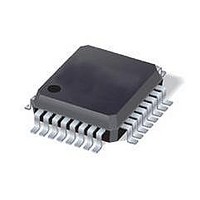
ST7FLITE49K2T6 STMicroelectronics, ST7FLITE49K2T6 Datasheet - Page 132

ST7FLITE49K2T6
Manufacturer Part Number
ST7FLITE49K2T6
Description
IC MCU 8BIT 8K FLASH 32LQFP
Manufacturer
STMicroelectronics
Series
ST7r
Datasheet
1.ST7FLITE49K2T6TR.pdf
(245 pages)
Specifications of ST7FLITE49K2T6
Core Processor
ST7
Core Size
8-Bit
Speed
8MHz
Connectivity
I²C, SPI
Peripherals
LVD, POR, PWM, WDT
Number Of I /o
24
Program Memory Size
8KB (8K x 8)
Program Memory Type
FLASH
Eeprom Size
256 x 8
Ram Size
384 x 8
Voltage - Supply (vcc/vdd)
2.4 V ~ 5.5 V
Data Converters
A/D 10x10b
Oscillator Type
Internal
Operating Temperature
-40°C ~ 85°C
Package / Case
32-LQFP
Processor Series
ST7FLITE4x
Core
ST7
Data Bus Width
8 bit
Data Ram Size
384 B
Interface Type
I2C, SPI
Maximum Clock Frequency
8 MHz
Number Of Programmable I/os
24
Number Of Timers
4
Maximum Operating Temperature
+ 85 C
Mounting Style
SMD/SMT
Development Tools By Supplier
ST7FLITE-SK/RAIS, ST7FLI49M-D/RAIS, STX-RLINK
Minimum Operating Temperature
- 40 C
On-chip Adc
10 bit, 10 Channel
For Use With
497-8399 - BOARD EVAL ST7LITE49M/STLED316S497-5858 - EVAL BOARD PLAYBACK ST7FLITE
Lead Free Status / RoHS Status
Lead free / RoHS Compliant
Available stocks
Company
Part Number
Manufacturer
Quantity
Price
Company:
Part Number:
ST7FLITE49K2T6
Manufacturer:
ST
Quantity:
3 000
Company:
Part Number:
ST7FLITE49K2T6
Manufacturer:
STMicroelectronics
Quantity:
10 000
Company:
Part Number:
ST7FLITE49K2T6TR
Manufacturer:
STMicroelectronics
Quantity:
10 000
On-chip peripherals
132/245
Bit 1 = IEDG1 Input edge 1
Bit 0 = OLVL1 Output level 1
Timer A
Reset value: 0000 0000 (00h)
Bit 7 = OC1E Output compare 1 pin enable
Bit 6 = 0C2E Output compare 2 pin enable
Bit 5 = OPM One pulse mode
Bit 4 = PWM Pulse width modulation
Bits 3:2 CC[1:0] Clock control
OC1E
This bit determines which type of level transition on the ICAP1 pin triggers the capture.
0: A falling edge triggers the capture
1: A rising edge triggers the capture
The OLVL1 bit is copied to the OCMP1 pin whenever a successful comparison occurs
with the OC1R register and the OC1E bit is set in the CR2 register.
This bit is used only to output the signal from the timer on the OCMP1 pin (OLV1 in
output compare mode, both OLV1 and OLV2 in PWM and one-pulse mode). Whatever
the value of the OC1E bit, the output compare 1 function of the timer remains active.
0: OCMP1 pin alternate function disabled (I/O pin free for general-purpose I/O)
1: OCMP1 pin alternate function enabled
This bit is used only to output the signal from the timer on the OCMP2 pin (OLV2 in
output compare mode). Whatever the value of the OC2E bit, the output compare 2
function of the timer remains active.
0: OCMP2 pin alternate function disabled (I/O pin free for general-purpose I/O)
1: OCMP2 pin alternate function enabled
0: One pulse mode is not active
1: One pulse mode is active, the ICAP1 pin can be used to trigger one pulse on
the OCMP1 pin; the active transition is given by the IEDG1 bit. The length of
the generated pulse depends on the contents of the OC1R register.
0: PWM mode is not active
1: PWM mode is active, the OCMP1 pin outputs a programmable cyclic signal;
the length of the pulse depends on the value of OC1R register; the period
depends on the value of OC2R register.
The timer clock mode depends on the following bits:
00: Timer clock = f
01: Timer clock = f
7
control register 2 (TACR2)
OC2E
CPU
CPU
OPM
/4
/2
PWM
Read / Write
CC[1:0]
IEDG2
ST7LITE49K2
EXEDG
0


