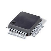
ST7FLITE49K2T6 STMicroelectronics, ST7FLITE49K2T6 Datasheet - Page 86

ST7FLITE49K2T6
Manufacturer Part Number
ST7FLITE49K2T6
Description
IC MCU 8BIT 8K FLASH 32LQFP
Manufacturer
STMicroelectronics
Series
ST7r
Datasheet
1.ST7FLITE49K2T6TR.pdf
(245 pages)
Specifications of ST7FLITE49K2T6
Core Processor
ST7
Core Size
8-Bit
Speed
8MHz
Connectivity
I²C, SPI
Peripherals
LVD, POR, PWM, WDT
Number Of I /o
24
Program Memory Size
8KB (8K x 8)
Program Memory Type
FLASH
Eeprom Size
256 x 8
Ram Size
384 x 8
Voltage - Supply (vcc/vdd)
2.4 V ~ 5.5 V
Data Converters
A/D 10x10b
Oscillator Type
Internal
Operating Temperature
-40°C ~ 85°C
Package / Case
32-LQFP
Processor Series
ST7FLITE4x
Core
ST7
Data Bus Width
8 bit
Data Ram Size
384 B
Interface Type
I2C, SPI
Maximum Clock Frequency
8 MHz
Number Of Programmable I/os
24
Number Of Timers
4
Maximum Operating Temperature
+ 85 C
Mounting Style
SMD/SMT
Development Tools By Supplier
ST7FLITE-SK/RAIS, ST7FLI49M-D/RAIS, STX-RLINK
Minimum Operating Temperature
- 40 C
On-chip Adc
10 bit, 10 Channel
For Use With
497-8399 - BOARD EVAL ST7LITE49M/STLED316S497-5858 - EVAL BOARD PLAYBACK ST7FLITE
Lead Free Status / RoHS Status
Lead free / RoHS Compliant
Available stocks
Company
Part Number
Manufacturer
Quantity
Price
Company:
Part Number:
ST7FLITE49K2T6
Manufacturer:
ST
Quantity:
3 000
Company:
Part Number:
ST7FLITE49K2T6
Manufacturer:
STMicroelectronics
Quantity:
10 000
Company:
Part Number:
ST7FLITE49K2T6TR
Manufacturer:
STMicroelectronics
Quantity:
10 000
On-chip peripherals
11.2.3
86/245
Functional description
PWM mode
This mode allows up to four Pulse Width Modulated signals to be generated on the PWMx
output pins.
●
●
PWM frequency
The four PWM signals can have the same frequency (f
frequencies. This is selected by the ENCNTR2 bit which enables Single Timer or Dual
Timer mode (see
period and the ATR register value. In Dual Timer mode, PWM2 and PWM3 can be
generated with a different frequency controlled by CNTR2 and ATR2.
Following the above formula, if f
2 MHz (ATR register value = 4094), and the minimum value is 1 kHz (ATR register
value = 0).
The maximum value of ATR is 4094 because it must be lower than the DC4R value
which must be 4095 in this case.
To update the DCRx registers at 32 MHz, the following precautions must be taken:
–
–
Duty cycle
The duty cycle is selected by programming the DCRx registers. These are preload
registers. The DCRx values are transferred in Active duty cycle registers after an
overflow event if the corresponding transfer bit (TRANx bit) is set.
The TRAN1 bit controls the PWMx outputs driven by counter 1 and the TRAN2 bit
controls the PWMx outputs driven by counter 2.
PWM generation and output compare are done by comparing these active DCRx
values with the counter.
The maximum available resolution for the PWMx duty cycle is:
where ATR is equal to 0. With this maximum resolution, 0% and 100% duty cycle can
be obtained by changing the polarity.
At reset, the counter starts counting from 0.
When a upcounter overflow occurs (OVF event), the preloaded Duty cycle values are
transferred to the active Duty Cycle registers and the PWMx signals are set to a high
level. When the upcounter matches the active DCRx value the PWMx signals are set to
a low level. To obtain a signal on a PWMx pin, the contents of the corresponding active
DCRx register must be greater than the contents of the ATR register.
If the PWM frequency is < 1 MHz and the TRANx bit is set asynchronously, it
should be set twice after a write to the DCRx registers.
If the PWM frequency is > 1 MHz, the TRANx bit should be set along with
FORCEx bit with the same instruction (use a load instruction and not 2 bset
instructions).
Figure 37
f
PWM
Resolution
and
=
COUNTER
Figure
f
COUNTER
=
38). The frequency is controlled by the counter
1
equals 4 MHz
⁄
⁄
(
4096 ATR
(
4096 ATR
–
–
PWM
,
)
the maximum value of f
)
) or can have two different
ST7LITE49K2
PWM
is


