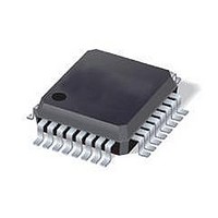
ST7FLITE49K2T6 STMicroelectronics, ST7FLITE49K2T6 Datasheet - Page 95

ST7FLITE49K2T6
Manufacturer Part Number
ST7FLITE49K2T6
Description
IC MCU 8BIT 8K FLASH 32LQFP
Manufacturer
STMicroelectronics
Series
ST7r
Datasheet
1.ST7FLITE49K2T6TR.pdf
(245 pages)
Specifications of ST7FLITE49K2T6
Core Processor
ST7
Core Size
8-Bit
Speed
8MHz
Connectivity
I²C, SPI
Peripherals
LVD, POR, PWM, WDT
Number Of I /o
24
Program Memory Size
8KB (8K x 8)
Program Memory Type
FLASH
Eeprom Size
256 x 8
Ram Size
384 x 8
Voltage - Supply (vcc/vdd)
2.4 V ~ 5.5 V
Data Converters
A/D 10x10b
Oscillator Type
Internal
Operating Temperature
-40°C ~ 85°C
Package / Case
32-LQFP
Processor Series
ST7FLITE4x
Core
ST7
Data Bus Width
8 bit
Data Ram Size
384 B
Interface Type
I2C, SPI
Maximum Clock Frequency
8 MHz
Number Of Programmable I/os
24
Number Of Timers
4
Maximum Operating Temperature
+ 85 C
Mounting Style
SMD/SMT
Development Tools By Supplier
ST7FLITE-SK/RAIS, ST7FLI49M-D/RAIS, STX-RLINK
Minimum Operating Temperature
- 40 C
On-chip Adc
10 bit, 10 Channel
For Use With
497-8399 - BOARD EVAL ST7LITE49M/STLED316S497-5858 - EVAL BOARD PLAYBACK ST7FLITE
Lead Free Status / RoHS Status
Lead free / RoHS Compliant
Available stocks
Company
Part Number
Manufacturer
Quantity
Price
Company:
Part Number:
ST7FLITE49K2T6
Manufacturer:
ST
Quantity:
3 000
Company:
Part Number:
ST7FLITE49K2T6
Manufacturer:
STMicroelectronics
Quantity:
10 000
Company:
Part Number:
ST7FLITE49K2T6TR
Manufacturer:
STMicroelectronics
Quantity:
10 000
ST7LITE49K2
On-chip peripherals
One pulse mode
One pulse mode can be used to control PWM2/3 signal with an external LTIC pin. This
mode is available only in Dual Timer mode i.e. only for CNTR2, when the OP_EN bit in
PWM3CSR register is set.
One Pulse mode is activated by the external LTIC input. The active edge of the LTIC pin is
selected by the OPEDGE bit in the PWM3CSR register.
After getting the active edge of the LTIC pin, CNTR2 is reset (000h) and PWM3 is set to
high. CNTR2 starts counting from 000h, when it reaches the active DCR3 value then PWM3
goes low. Till this time, any further transitions on the LTIC signal will have no effect. If there
are LTIC transitions after CNTR2 reaches DCR3 value, CNTR2 is reset again and PWM3
goes high.
If there is no LTIC active edge, CNTR2 counts until it reaches the ATR2 value, then it is reset
again and PWM3 is set to high. The counter again starts counting from 000h, when it
reaches the active DCR3 value PWM3 goes low, the counter counts until it reaches ATR2, it
resets and PWM3 is set to high and so on.
The same operation applies for PWM2, but in this case the comparison is done on DCR2.
OP_EN and OPEDGE bits take effect on the fly and are not synchronized with Counter 2
overflow. The output bit OP2/3 can be used to inverse the polarity of PWM2/3 in one-pulse
mode. The update of these bits (OP2/3) is synchronized with the counter 2 overflow, they
will be updated if the TRAN2 bit is set.
The time taken from activation of LTIC input and CNTR2 reset is between 2 and 3 t
CNTR2
cycles, that is, from around 62.5 ns to 94 ns (at 32 MHz input frequency).
Lite timer Input Capture interrupt should be disabled while 12-bit ARtimer is in One Pulse
mode. This is to avoid spurious interrupts.
The priority of the various conditions for PWM3 is the following: Break > one-pulse mode
with active LTIC edge > Forced overflow by s/w > one-pulse mode without active LTIC edge
> normal PWM operation.
It is possible to update DCR2/3 and OP2/3 at the counter 2 reset, the update is
synchronized with the counter reset. This is managed by the overflow interrupt which is
generated if counter is reset either due to ATR match or active pulse at LTIC pin. DCR2/3
and OP2/3 update in one-pulse mode is performed dynamically using a software force
update. DCR3 update in this mode is not synchronized with any event. That may lead to a
longer next PWM3 cycle duration than expected just after the change.
In One Pulse mode ATR2 value must be greater than DCR2/3 value for PWM2/3. (opposite
to normal PWM mode).
If there is an active edge on the LTIC pin after the counter has reset due to an ATR2 match,
then the timer again gets reset and appears as modified Duty cycle depending on whether
the new DCR value is less than or more than the previous value.
The TRAN2 bit should be set along with the FORCE2 bit with the same instruction after a
write to the DCR register.
ATR2 value should be changed after an overflow in one pulse mode to avoid any irregular
PWM cycle.
When exiting from one pulse mode, the OP_EN bit in the PWM3CSR register should be
reset first and then the ENCNTR2 bit (if counter 2 must be stopped).
95/245


