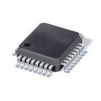
C8051F352-GQR Silicon Laboratories Inc, C8051F352-GQR Datasheet - Page 113

C8051F352-GQR
Manufacturer Part Number
C8051F352-GQR
Description
IC 8051 MCU 8K FLASH 32LQFP
Manufacturer
Silicon Laboratories Inc
Series
C8051F35xr
Specifications of C8051F352-GQR
Core Processor
8051
Core Size
8-Bit
Speed
50MHz
Connectivity
SMBus (2-Wire/I²C), SPI, UART/USART
Peripherals
POR, PWM, Temp Sensor, WDT
Number Of I /o
17
Program Memory Size
8KB (8K x 8)
Program Memory Type
FLASH
Ram Size
768 x 8
Voltage - Supply (vcc/vdd)
2.7 V ~ 3.6 V
Data Converters
A/D 8x16b; D/A 2x8b
Oscillator Type
Internal
Operating Temperature
-40°C ~ 85°C
Package / Case
32-LQFP
Core
8051
Processor Series
C8051F3x
Data Bus Width
8 bit
Maximum Clock Frequency
50 MHz
Data Ram Size
768 B
Data Rom Size
128 B
On-chip Adc
Yes
Number Of Programmable I/os
17
Number Of Timers
4 bit
Operating Supply Voltage
2.7 V to 3.6 V
Mounting Style
SMD/SMT
A/d Bit Size
16 bit
A/d Channels Available
8
Height
1.4 mm
Interface Type
I2C, SMBus, SPI, UART
Length
7 mm
Maximum Operating Temperature
+ 85 C
Minimum Operating Temperature
- 40 C
Supply Voltage (max)
3.6 V
Supply Voltage (min)
2.7 V
Width
7 mm
For Use With
336-1083 - DEV KIT FOR F350/351/352/353
Lead Free Status / RoHS Status
Lead free / RoHS Compliant
Eeprom Size
-
Lead Free Status / Rohs Status
Details
Available stocks
Company
Part Number
Manufacturer
Quantity
Price
Company:
Part Number:
C8051F352-GQR
Manufacturer:
Silicon Laboratories Inc
Quantity:
10 000
Company:
Part Number:
C8051F352-GQR..
Manufacturer:
SILICON
Quantity:
15 000
13. Prefetch Engine
The C8051F350/1/2/3 family of devices incorporate a 2-byte prefetch engine. Because the access time of
the Flash memory is 40 ns, and the minimum instruction time is 20 ns, the prefetch engine is necessary for
full-speed code execution. Instructions are read from Flash memory two bytes at a time by the prefetch
engine, and given to the CIP-51 processor core to execute. When running linear code (code without any
jumps or branches), the prefetch engine allows instructions to be executed at full speed. When a code
branch occurs, the processor may be stalled for up to two clock cycles while the next set of code bytes is
retrieved from Flash memory. The FLRT bit (FLSCL.4) determines how many clock cycles are used to read
each set of two code bytes from Flash. When operating from a system clock of 25 MHz or less, the FLRT
bit should be set to ‘0’ so that the prefetch engine takes only one clock cycle for each read. When operat-
ing with a system clock of greater than 25 MHz (up to 50 MHz), the FLRT bit should be set to ‘1’, so that
each prefetch code read lasts for two clock cycles.
Bits 7–6: Unused. Read = 00b; Write = Don’t Care
Bit 5:
Bits 4–1: Unused. Read = 0000b; Write = Don’t Care
Bit 0:
Bit7
R
PFEN: Prefetch Enable.
This bit enables the prefetch engine.
0: Prefetch engine is disabled.
1: Prefetch engine is enabled.
FLBWE: Flash Block Write Enable.
This bit allows block writes to Flash memory from software.
0: Each byte of a software Flash write is written individually.
1: Flash bytes are written in groups of two.
Bit6
SFR Definition 13.1. PFE0CN: Prefetch Engine Control
R
PFEN
R/W
Bit5
Bit4
R
Rev. 1.1
Bit3
R
Bit2
R
C8051F350/1/2/3
Bit1
R
SFR Address: 0xE3
FLBWE
R/W
Bit0
00100000
Reset Value
113


