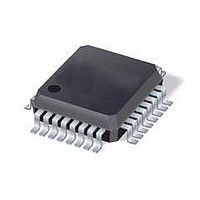
C8051F352-GQR Silicon Laboratories Inc, C8051F352-GQR Datasheet - Page 46

C8051F352-GQR
Manufacturer Part Number
C8051F352-GQR
Description
IC 8051 MCU 8K FLASH 32LQFP
Manufacturer
Silicon Laboratories Inc
Series
C8051F35xr
Specifications of C8051F352-GQR
Core Processor
8051
Core Size
8-Bit
Speed
50MHz
Connectivity
SMBus (2-Wire/I²C), SPI, UART/USART
Peripherals
POR, PWM, Temp Sensor, WDT
Number Of I /o
17
Program Memory Size
8KB (8K x 8)
Program Memory Type
FLASH
Ram Size
768 x 8
Voltage - Supply (vcc/vdd)
2.7 V ~ 3.6 V
Data Converters
A/D 8x16b; D/A 2x8b
Oscillator Type
Internal
Operating Temperature
-40°C ~ 85°C
Package / Case
32-LQFP
Core
8051
Processor Series
C8051F3x
Data Bus Width
8 bit
Maximum Clock Frequency
50 MHz
Data Ram Size
768 B
Data Rom Size
128 B
On-chip Adc
Yes
Number Of Programmable I/os
17
Number Of Timers
4 bit
Operating Supply Voltage
2.7 V to 3.6 V
Mounting Style
SMD/SMT
A/d Bit Size
16 bit
A/d Channels Available
8
Height
1.4 mm
Interface Type
I2C, SMBus, SPI, UART
Length
7 mm
Maximum Operating Temperature
+ 85 C
Minimum Operating Temperature
- 40 C
Supply Voltage (max)
3.6 V
Supply Voltage (min)
2.7 V
Width
7 mm
For Use With
336-1083 - DEV KIT FOR F350/351/352/353
Lead Free Status / RoHS Status
Lead free / RoHS Compliant
Eeprom Size
-
Lead Free Status / Rohs Status
Details
Available stocks
Company
Part Number
Manufacturer
Quantity
Price
Company:
Part Number:
C8051F352-GQR
Manufacturer:
Silicon Laboratories Inc
Quantity:
10 000
Company:
Part Number:
C8051F352-GQR..
Manufacturer:
SILICON
Quantity:
15 000
C8051F350/1/2/3
5.3.
Performing Conversions
The ADC offers two conversion modes: Single Conversion, and Continuous Conversion. In single conver-
sion mode, a single conversion result is produced for each of the filters (SINC3 and Fast). In continuous
conversion mode, the ADC will perform back-to-back conversions until the ADC mode is changed. Proce-
dures for single and continuous conversion modes are detailed in the sections below.
5.3.1. Single Conversions
A single conversion is initiated by writing the ADC System Mode bits (AD0SM) to the “Single Conversion”
option. Single conversion mode instructs the ADC to gather enough information to produce a result for the
filter that is selected by the AD0ISEL bit. During the conversion, the AD0BUSY flag will be set to ‘1’. The
Fast filter results will be available after one period of the ADC’s conversion cycle (determined by the mod-
ulator clock and the decimation ratio). The SINC3 filter results will be available after three periods of the
ADC’s conversion cycle. The AD0ISEL bit in register ADC0CF determines when the end-of-conversion
interrupt will occur, and return the ADC to Idle mode. If the AD0ISEL bit is set to ‘1’, the AD0INT bit will be
set to ‘1’ when the Fast filter results are available. If the AD0ISEL bit is cleared to ‘0’, the AD0INT bit will be
set to ‘1’ when the SINC3 filter results are available. The AD0SM bits will return to idle mode and the
AD0BUSY bit will be cleared to ‘0’ when the selected filter is finished. When using the SINC3 filter, a valid
result will also be output by the Fast filter. When using the Fast filter in single-conversion mode, the SINC3
filter results will not be accurate.
5.3.2. Continuous Conversions
Continuous conversions are initiated by writing the ADC System Mode bits (AD0SM) to the “Continuous
Conversion” option. In continous conversion mode, the ADC will start a new conversion as soon as each
conversion is completed. During the conversions, the AD0BUSY flag will be set to ‘1’. The Fast filter results
will be available after one period of the ADC’s conversion cycle, and on every conversion cycle thereafter
(determined by the modulator clock and the decimation ratio). The first SINC3 filter result will be available
after three periods of the ADC’s conversion cycle, and subsequent SINC3 conversion results will be avail-
able at the end of every conversion cycle thereafter. The AD0ISEL bit in register ADC0CF determines
when the end-of-conversion interrupts will occur. If the AD0ISEL bit is cleared to ‘0’, the AD0INT bit will be
set to ‘1’ when SINC3 filter results are available. If the AD0ISEL bit is set to ‘1’, the AD0INT bit will be set to
‘1’ when Fast filter results are available. Regardless of the setting of the AD0ISEL bit, both filters will
update their results registers when new results are available. To stop conversions and exit from continuous
conversion mode, the AD0SM bits should be written to Idle mode.
5.3.3. ADC Output
The ADC’s two filters each have their own output data registers. The SINC3 filter results are stored in the
ADC0H, ADC0M, and ADC0L registers, while the Fast filter results are stored in the ADC0FH, ADC0FM,
and ADC0FL registers. The ADC output can be configured for Unipolar or Bipolar mode using the AD0POL
bit in register ADC0CN. Decoding of the ADC output words are shown in Table 5.1 and Table 5.2. The
SINC3 filter uses information from the past three conversion cycles to produce an ADC output. The Fast fil-
ter uses information from only the current conversion cycle to produce an ADC output. The fast filter reacts
more quickly to changes on the analog input, while the SINC3 filter produces lower-noise results.
46
Rev. 1.1


