C8051F352-GQR Silicon Laboratories Inc, C8051F352-GQR Datasheet - Page 99
C8051F352-GQR
Manufacturer Part Number
C8051F352-GQR
Description
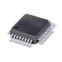
IC 8051 MCU 8K FLASH 32LQFP
Manufacturer
Silicon Laboratories Inc
Series
C8051F35xr
Specifications of C8051F352-GQR
Core Processor
8051
Core Size
8-Bit
Speed
50MHz
Connectivity
SMBus (2-Wire/I²C), SPI, UART/USART
Peripherals
POR, PWM, Temp Sensor, WDT
Number Of I /o
17
Program Memory Size
8KB (8K x 8)
Program Memory Type
FLASH
Ram Size
768 x 8
Voltage - Supply (vcc/vdd)
2.7 V ~ 3.6 V
Data Converters
A/D 8x16b; D/A 2x8b
Oscillator Type
Internal
Operating Temperature
-40°C ~ 85°C
Package / Case
32-LQFP
Core
8051
Processor Series
C8051F3x
Data Bus Width
8 bit
Maximum Clock Frequency
50 MHz
Data Ram Size
768 B
Data Rom Size
128 B
On-chip Adc
Yes
Number Of Programmable I/os
17
Number Of Timers
4 bit
Operating Supply Voltage
2.7 V to 3.6 V
Mounting Style
SMD/SMT
A/d Bit Size
16 bit
A/d Channels Available
8
Height
1.4 mm
Interface Type
I2C, SMBus, SPI, UART
Length
7 mm
Maximum Operating Temperature
+ 85 C
Minimum Operating Temperature
- 40 C
Supply Voltage (max)
3.6 V
Supply Voltage (min)
2.7 V
Width
7 mm
For Use With
336-1083 - DEV KIT FOR F350/351/352/353
Lead Free Status / RoHS Status
Lead free / RoHS Compliant
Eeprom Size
-
Lead Free Status / Rohs Status
Details
Available stocks
Company
Part Number
Manufacturer
Quantity
Price
Company:

Part Number:
C8051F352-GQR
Manufacturer:
Silicon Laboratories Inc
Quantity:
10 000
Company:
Part Number:
C8051F352-GQR..
Manufacturer:
SILICON
Quantity:
15 000


11. Memory Organization and SFRs
The memory organization of the C8051F350/1/2/3 is similar to that of a standard 8051. There are two sep-
arate memory spaces: program memory and data memory. Program and data memory share the same
address space but are accessed via different instruction types. The memory map is shown in Figure 11.1.
11.1. Program Memory
The CIP-51 core has a 64 kB program memory space. The C8051F350/1/2/3 implements 8 kB of this pro-
gram memory space as in-system, re-programmable Flash memory, organized in a contiguous block from
addresses 0x0000 to 0x1DFF. Addresses above 0x1DFF are reserved.
Program memory is normally assumed to be read-only. However, the C8051F350/1/2/3 can write to pro-
gram memory by setting the Program Store Write Enable bit (PSCTL.0) and using the MOVX write instruc-
tion. This feature provides a mechanism for updates to program code and use of the program memory
space for non-volatile data storage. Refer to Section “15. Flash Memory’ on page 121 for further details.
0x1DFF
0x1FFF
0x1E00
0x0000
PROGRAM/DATA MEMORY
Programmable in 512
Byte Sectors)
RESERVED
(In-System
8 kB Flash
(Flash)
Figure 11.1. Memory Map
0xFFFF
0x01FF
0x0200
0x0000
0xFF
0x7F
0x2F
0x1F
0x80
0x30
0x20
0x00
Rev. 1.1
0x0000 to 0x01FF, wrapped
XRAM - 512 Bytes
(accessable using MOVX
Same 512 bytes as from
(Indirect Addressing
on 512-byte boundaries
(Direct and Indirect
INTERNAL DATA ADDRESS SPACE
EXTERNAL DATA ADDRESS SPACE
General Purpose
Upper 128 RAM
Bit Addressable
Addressing)
instruction)
Registers
Only)
DATA MEMORY (RAM)
C8051F350/1/2/3
(Direct Addressing Only)
Special Function
Lower 128 RAM
(Direct and Indirect
Addressing)
Register's
99
Related parts for C8051F352-GQR
Image
Part Number
Description
Manufacturer
Datasheet
Request
R

Part Number:
Description:
SMD/C°/SINGLE-ENDED OUTPUT SILICON OSCILLATOR
Manufacturer:
Silicon Laboratories Inc
Part Number:
Description:
Manufacturer:
Silicon Laboratories Inc
Datasheet:
Part Number:
Description:
N/A N/A/SI4010 AES KEYFOB DEMO WITH LCD RX
Manufacturer:
Silicon Laboratories Inc
Datasheet:
Part Number:
Description:
N/A N/A/SI4010 SIMPLIFIED KEY FOB DEMO WITH LED RX
Manufacturer:
Silicon Laboratories Inc
Datasheet:
Part Number:
Description:
N/A/-40 TO 85 OC/EZLINK MODULE; F930/4432 HIGH BAND (REV E/B1)
Manufacturer:
Silicon Laboratories Inc
Part Number:
Description:
EZLink Module; F930/4432 Low Band (rev e/B1)
Manufacturer:
Silicon Laboratories Inc
Part Number:
Description:
I°/4460 10 DBM RADIO TEST CARD 434 MHZ
Manufacturer:
Silicon Laboratories Inc
Part Number:
Description:
I°/4461 14 DBM RADIO TEST CARD 868 MHZ
Manufacturer:
Silicon Laboratories Inc
Part Number:
Description:
I°/4463 20 DBM RFSWITCH RADIO TEST CARD 460 MHZ
Manufacturer:
Silicon Laboratories Inc
Part Number:
Description:
I°/4463 20 DBM RADIO TEST CARD 868 MHZ
Manufacturer:
Silicon Laboratories Inc
Part Number:
Description:
I°/4463 27 DBM RADIO TEST CARD 868 MHZ
Manufacturer:
Silicon Laboratories Inc
Part Number:
Description:
I°/4463 SKYWORKS 30 DBM RADIO TEST CARD 915 MHZ
Manufacturer:
Silicon Laboratories Inc
Part Number:
Description:
N/A N/A/-40 TO 85 OC/4463 RFMD 30 DBM RADIO TEST CARD 915 MHZ
Manufacturer:
Silicon Laboratories Inc
Part Number:
Description:
I°/4463 20 DBM RADIO TEST CARD 169 MHZ
Manufacturer:
Silicon Laboratories Inc