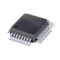
C8051F352-GQR Silicon Laboratories Inc, C8051F352-GQR Datasheet - Page 73

C8051F352-GQR
Manufacturer Part Number
C8051F352-GQR
Description
IC 8051 MCU 8K FLASH 32LQFP
Manufacturer
Silicon Laboratories Inc
Series
C8051F35xr
Specifications of C8051F352-GQR
Core Processor
8051
Core Size
8-Bit
Speed
50MHz
Connectivity
SMBus (2-Wire/I²C), SPI, UART/USART
Peripherals
POR, PWM, Temp Sensor, WDT
Number Of I /o
17
Program Memory Size
8KB (8K x 8)
Program Memory Type
FLASH
Ram Size
768 x 8
Voltage - Supply (vcc/vdd)
2.7 V ~ 3.6 V
Data Converters
A/D 8x16b; D/A 2x8b
Oscillator Type
Internal
Operating Temperature
-40°C ~ 85°C
Package / Case
32-LQFP
Core
8051
Processor Series
C8051F3x
Data Bus Width
8 bit
Maximum Clock Frequency
50 MHz
Data Ram Size
768 B
Data Rom Size
128 B
On-chip Adc
Yes
Number Of Programmable I/os
17
Number Of Timers
4 bit
Operating Supply Voltage
2.7 V to 3.6 V
Mounting Style
SMD/SMT
A/d Bit Size
16 bit
A/d Channels Available
8
Height
1.4 mm
Interface Type
I2C, SMBus, SPI, UART
Length
7 mm
Maximum Operating Temperature
+ 85 C
Minimum Operating Temperature
- 40 C
Supply Voltage (max)
3.6 V
Supply Voltage (min)
2.7 V
Width
7 mm
For Use With
336-1083 - DEV KIT FOR F350/351/352/353
Lead Free Status / RoHS Status
Lead free / RoHS Compliant
Eeprom Size
-
Lead Free Status / Rohs Status
Details
Available stocks
Company
Part Number
Manufacturer
Quantity
Price
Company:
Part Number:
C8051F352-GQR
Manufacturer:
Silicon Laboratories Inc
Quantity:
10 000
Company:
Part Number:
C8051F352-GQR..
Manufacturer:
SILICON
Quantity:
15 000
7.
There are two voltage reference options for the C8051F350/1/2/3 ADCs: the internal 2.5 V reference volt-
age, or an external reference voltage (see Figure 7.1). The AD0VREF bit in the ADC0CF register selects
the reference source.
The internal voltage reference circuit consists of a 1.25 V, temperature stable bandgap voltage reference
generator and a gain-of-two output buffer amplifier, to produce a 2.5 V voltage reference. When the inter-
nal voltage reference is used, it is driven out on the VREF+ pin. In this configuration, the VREF– must be
connected to the AGND pin external to the device. See Section “24. Revision Specific Behavior’ on
page 227 for more information. The internal voltage reference is enabled by setting the AD0EN bit in regis-
ter ADC0MD to ‘1’ and clearing the AD0VREF bit in register ADC0CF to ‘0’ (See Section “5. 24 or 16-Bit
Analog to Digital Converter (ADC0)’ on page 41). Electrical specifications for the internal voltage reference
and bias generators are given in Table 7.1.
The internal oscillator bias generator is automatically enabled whenever the internal oscillator is enabled.
For power requirement characterization, the BIASE bit in register REF0CN can also be used to enable the
internal oscillator bias generator, when the oscillator itself is not enabled. Likewise, the REFBE bit in regis-
ter REF0CN can be used to enable the internal bandgap generator, which is used by the ADC, the IDACs,
the Clock Multiplier, and the internal Voltage Reference. The internal reference bias generator is automati-
cally enabled whenever a peripheral requires it. See SFR Definition 7.1 for the REF0CN register descrip-
tion.
Reference
(Optional)
External
Voltage
Voltage Reference
(Recommended)
Capacitors
Bypass
+
Figure 7.1. Reference Circuitry Block Diagram
VREF+
VREF–
REFBE
BIASE
AD0VREF
AD0EN
IOSCEN
IDA0EN
IDA1EN
MULEN
AD0EN
Rev. 1.1
VREF to ADC
EN
EN
C8051F350/1/2/3
EN
Bias Generator
Oscillator Bias
Generator
Reference
Reference
Internal
Internal
Buffer
2.5 V
To Internal
Oscillator
To ADC, IDACs,
Clock Multiplier
73


