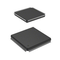
HD6417750RF240DV Renesas Electronics America, HD6417750RF240DV Datasheet - Page 229

HD6417750RF240DV
Manufacturer Part Number
HD6417750RF240DV
Description
MPU 3V 16K I-TEMP,PB-FREE 208-QF
Manufacturer
Renesas Electronics America
Series
SuperH® SH7750r
Datasheet
1.D6417750RBP240DV.pdf
(1164 pages)
Specifications of HD6417750RF240DV
Core Processor
SH-4
Core Size
32-Bit
Speed
240MHz
Connectivity
EBI/EMI, FIFO, SCI, SmartCard
Peripherals
DMA, POR, WDT
Number Of I /o
28
Program Memory Type
ROMless
Ram Size
48K x 8
Voltage - Supply (vcc/vdd)
1.4 V ~ 1.6 V
Oscillator Type
External
Operating Temperature
-40°C ~ 85°C
Package / Case
208-QFP
Lead Free Status / RoHS Status
Lead free / RoHS Compliant
Eeprom Size
-
Program Memory Size
-
Data Converters
-
Available stocks
Company
Part Number
Manufacturer
Quantity
Price
Company:
Part Number:
HD6417750RF240DV
Manufacturer:
HITACHI
Quantity:
7 287
- Current page: 229 of 1164
- Download datasheet (7Mb)
4.7.2
A write to the SQs can be performed using a store instruction (MOV) on P4 area H'E000 0000 to
H'E3FF FFFC. A longword or quadword access size can be used. The meaning of the address bits
is as follows:
[31:26]:
[25:6]:
[5]:
[4:2]:
[1:0]
4.7.3
Transfer from the SQs to external memory can be performed with a prefetch instruction (PREF).
Issuing a PREF instruction for P4 area H'E000 0000 to H'E3FF FFFC starts a burst transfer from
the SQs to external memory. The burst transfer length is fixed at 32 bytes, and the start address is
always at a 32-byte boundary. While the contents of one SQ are being transferred to external
memory, the other SQ can be written to without a penalty cycle, but writing to the SQ involved in
the transfer to external memory is deferred until the transfer is completed.
The SQ transfer destination external memory address bit [28:0] specification is as shown below,
according to whether the MMU is on or off.
• When MMU is on
The SQ area (H'E000 0000 to H'E3FF FFFF) is set in VPN of the UTLB, and the transfer
destination external memory address in PPN. The ASID, V, SZ, SH, PR, and D bits have the
same meaning as for normal address translation, but the C and WT bits have no meaning with
regard to this page. Since burst transfer is prohibited for PCMCIA areas, the SA and TC bits
also have no meaning.
SQ0
SQ1
SQ Writes
Transfer to External Memory
111000
Don't care
0/1
LW specification
00
SQ0[0]
SQ1[0]
4B
SQ0[1]
SQ1[1]
4B
Figure 4.16 Store Queue Configuration
Used for external memory transfer/access right
0: SQ0 specification
Fixed at 0
Store queue specification
Specifies longword position in SQ0/SQ1
SQ0[2]
SQ1[2]
4B
SQ0[3]
SQ1[3]
4B
SQ0[4]
SQ1[4]
4B
Rev.7.00 Oct. 10, 2008 Page 143 of 1074
1: SQ1 specification
SQ0[5]
SQ1[5]
4B
SQ0[6]
SQ1[6]
4B
REJ09B0366-0700
Section 4 Caches
SQ0[7]
SQ1[7]
4B
Related parts for HD6417750RF240DV
Image
Part Number
Description
Manufacturer
Datasheet
Request
R

Part Number:
Description:
KIT STARTER FOR M16C/29
Manufacturer:
Renesas Electronics America
Datasheet:

Part Number:
Description:
KIT STARTER FOR R8C/2D
Manufacturer:
Renesas Electronics America
Datasheet:

Part Number:
Description:
R0K33062P STARTER KIT
Manufacturer:
Renesas Electronics America
Datasheet:

Part Number:
Description:
KIT STARTER FOR R8C/23 E8A
Manufacturer:
Renesas Electronics America
Datasheet:

Part Number:
Description:
KIT STARTER FOR R8C/25
Manufacturer:
Renesas Electronics America
Datasheet:

Part Number:
Description:
KIT STARTER H8S2456 SHARPE DSPLY
Manufacturer:
Renesas Electronics America
Datasheet:

Part Number:
Description:
KIT STARTER FOR R8C38C
Manufacturer:
Renesas Electronics America
Datasheet:

Part Number:
Description:
KIT STARTER FOR R8C35C
Manufacturer:
Renesas Electronics America
Datasheet:

Part Number:
Description:
KIT STARTER FOR R8CL3AC+LCD APPS
Manufacturer:
Renesas Electronics America
Datasheet:

Part Number:
Description:
KIT STARTER FOR RX610
Manufacturer:
Renesas Electronics America
Datasheet:

Part Number:
Description:
KIT STARTER FOR R32C/118
Manufacturer:
Renesas Electronics America
Datasheet:

Part Number:
Description:
KIT DEV RSK-R8C/26-29
Manufacturer:
Renesas Electronics America
Datasheet:

Part Number:
Description:
KIT STARTER FOR SH7124
Manufacturer:
Renesas Electronics America
Datasheet:

Part Number:
Description:
KIT STARTER FOR H8SX/1622
Manufacturer:
Renesas Electronics America
Datasheet:

Part Number:
Description:
KIT DEV FOR SH7203
Manufacturer:
Renesas Electronics America
Datasheet:


