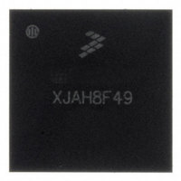
MC13224V Freescale Semiconductor, MC13224V Datasheet - Page 26

MC13224V
Manufacturer Part Number
MC13224V
Description
ZIGBEE PLATFORM 802.15.4 145-LGA
Manufacturer
Freescale Semiconductor
Datasheet
1.1322XUSB.pdf
(54 pages)
Specifications of MC13224V
Frequency
2.4GHz
Data Rate - Maximum
250kbps
Modulation Or Protocol
802.15.4 Zigbee
Applications
General Purpose
Power - Output
4dBm
Sensitivity
-100dBm
Voltage - Supply
2 V ~ 3.6 V
Current - Receiving
24mA
Current - Transmitting
29mA
Data Interface
PCB, Surface Mount
Memory Size
128kB Flash, 96kB RAM
Antenna Connector
PCB, Surface Mount
Operating Temperature
-40°C ~ 105°C
Package / Case
145-LGA
Number Of Receivers
1
Number Of Transmitters
1
Wireless Frequency
2.4 GHz
Interface Type
4-Wire SPI, I2C
Output Power
1.5 dBm
Operating Supply Voltage
2 V to 3.6 V
Maximum Operating Temperature
+ 105 C
Mounting Style
SMD/SMT
Maximum Supply Current
31 mA
Minimum Operating Temperature
- 40 C
Modulation
OQPSK
Protocol Supported
802.15.4
No. Of Pins
99
Supply Voltage Range
2V To 3.6V
Operating Temperature Range
-40°C To +125°C
Msl
MSL 3 - 168 Hours
A/d Converter
12 Bits
No. Of Timers 8/12/16/32 Bits
0 / 0 / 4 / 0
Rohs Compliant
Yes
Lead Free Status / RoHS Status
Lead free / RoHS Compliant
Available stocks
Company
Part Number
Manufacturer
Quantity
Price
Company:
Part Number:
MC13224V
Manufacturer:
Freescale Semiconductor
Quantity:
1 849
Company:
Part Number:
MC13224VR2
Manufacturer:
EPCOS
Quantity:
34 000
5.8
The MC1322x ADC module provides two 12-bit analog-to-digital converters (ADC_1 and ADC_2) with
eight external channels (ADC7 - ADC0) that can be multiplexed to either ADC. ADC_1 can also sample
a battery reference voltage for monitoring purposes. External pins (ADC2_VREFH, ADC2_VREFL,
ADC1_VREFH, and ADC1_VREFL) are provided for independent ADC reference voltages. The
minimum sample time is 20 µs.
Each ADC can be programmed to scan multiple selected channels on a timed basis. The primary clock to
the ADC module is the peripheral reference clock (typically 24 MHz). For the time period between scan
sequences, the primary clock is first divided by an 8-bit prescale (1-255), and the derived clock drives both
the 32-bit delay timer and the ADC sequencer. Each ADC has its own delay timer and sequencer.
Once a scan sequence has been initiated, all selected channels can be sampled. Registers are provided to
define thresholds that can be enabled for the sampled channels. A threshold can be assigned to a specific
channel and can be programmed to be a less-than or greater-than threshold. Multiple thresholds can be
assigned to a single channel. Warm-up of the analog portion of the ADC circuitry is provided for power
management, and a separate 300 kHz ADC clock must be programmed via its own divider.
The battery monitor has two (2) dedicated threshold registers to set the high and low limits of the battery
sample channel.
Sample values are stored in a 8x16-bit FIFO. The FIFO accumulates samples from both ADCs, and the
12-bit sample value and a 4-bit channel tag are saved for each sample. The FIFO is read by the CPU from
a register address.
The module can be programmed to interrupt the processor based on the timed sample activity. Sample
activity, sequencer activity, or FIFO “fullness” can all be enabled to generate an interrupt.
The ADCs can also be overridden to sample on command as opposed to sequencer, time-based activity.
26
D A TA
R eference C lock
M C U
B U S
Analog-to-Digital Converter (ADC) Module
P eripheral
R eg isters
P rescaler
C ontro l
32-B it
T im er
C om pare
D ivider
32-B it
Tim er
Figure 8
Figure 8. ADC Module Block Diagram
S equ encer
S equ encer
MC1322x Technical Data, Rev. 1.3
300 kH z
O verride
O verride
C o ntrol
C o ntrol
M o de
M o de
1
b it channel
2
shows a block diagram of the ADC module.
(8 x 16-B it,
valu e + 4-
12-bit
F IFO
Tag)
A D C 2 E nable
A D C 1 E nable
M
U
X
M
U
X
A D C 1 M ux S el
A D C _1
A D C _2
A D C 2 M ux S el
B attery
M
M
U
X
U
X
A nalog
Freescale Semiconductor
A n alog C h ann els
A D C 0 - A D C 7


