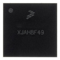
MC13224V Freescale Semiconductor, MC13224V Datasheet - Page 46

MC13224V
Manufacturer Part Number
MC13224V
Description
ZIGBEE PLATFORM 802.15.4 145-LGA
Manufacturer
Freescale Semiconductor
Datasheet
1.1322XUSB.pdf
(54 pages)
Specifications of MC13224V
Frequency
2.4GHz
Data Rate - Maximum
250kbps
Modulation Or Protocol
802.15.4 Zigbee
Applications
General Purpose
Power - Output
4dBm
Sensitivity
-100dBm
Voltage - Supply
2 V ~ 3.6 V
Current - Receiving
24mA
Current - Transmitting
29mA
Data Interface
PCB, Surface Mount
Memory Size
128kB Flash, 96kB RAM
Antenna Connector
PCB, Surface Mount
Operating Temperature
-40°C ~ 105°C
Package / Case
145-LGA
Number Of Receivers
1
Number Of Transmitters
1
Wireless Frequency
2.4 GHz
Interface Type
4-Wire SPI, I2C
Output Power
1.5 dBm
Operating Supply Voltage
2 V to 3.6 V
Maximum Operating Temperature
+ 105 C
Mounting Style
SMD/SMT
Maximum Supply Current
31 mA
Minimum Operating Temperature
- 40 C
Modulation
OQPSK
Protocol Supported
802.15.4
No. Of Pins
99
Supply Voltage Range
2V To 3.6V
Operating Temperature Range
-40°C To +125°C
Msl
MSL 3 - 168 Hours
A/d Converter
12 Bits
No. Of Timers 8/12/16/32 Bits
0 / 0 / 4 / 0
Rohs Compliant
Yes
Lead Free Status / RoHS Status
Lead free / RoHS Compliant
Available stocks
Company
Part Number
Manufacturer
Quantity
Price
Company:
Part Number:
MC13224V
Manufacturer:
Freescale Semiconductor
Quantity:
1 849
Company:
Part Number:
MC13224VR2
Manufacturer:
EPCOS
Quantity:
34 000
46
1
2
signal) to bridge the undefined region of the falling edge of SCL.
3
4
must then be met. This will automatically be the case if the device does not stretch the LOW period of the SCL signal.
If such a device does stretch the LOW period of the SCL signal, it must output the next data bit to the SDA line t
+ t
released.
5
SCL clock frequency (when source)
Hold time (repeated) START condition.
After this period, the first clock pulse is generated
LOW period of the SCL clock
HIGH period of the SCL clock
Set-up time for a repeated START condition
Data hold time
Data setup time
Rise time for both SDA and SCL signals
Fall time for both SDA and SCL signals
Bus free time between a STOP and START condition
Capacitive load for each bus line
All values referred to V
A device must internally provide a hold time of at least 300 ns for the SDA signal (referred to the V
The maximum t
A Fast-mode I2C-bus device can be used in a Standard-mode I2C-bus system, but the requirement t
SU;DAT
C
b
= total capacitance of one bus line in pF. If mixed with Hs-mode devices, the faster fall-times are allowed.
= 1000 + 250 = 1250 ns (according to the Standard-mode I2C-bus specification) before the SCL line is
HD;DAT
IHmin
has only to be met if the device does not stretch the LOW period (t
Parameter
and V
ILmax
Table 20. I
levels
MC1322x Technical Data, Rev. 1.3
2
C Signal AC Specifications
t
Symbol
t
SHD;DAT
t
t
HD;STA
SU:DAT
SU;STA
t
t
f
t
HIGH
LOW
SCL
BUF
C
t
t
r
f
b
Standard-Mode
Min
250
4.0
4.7
4.0
4.7
4.7
0
0
-
-
-
2
1
3.45
1000
Max
100
300
400
-
-
-
-
-
-
LOW
3
) of the SCL signal.
0.1C
0.1C
100
20 +
20 +
Min
0.6
1.3
0.6
0.6
1.3
0
Fast-Mode
0
-
IHmin
Freescale Semiconductor
2
4
b
b
SU;DAT
5
5
of the SCL
Max
0.9
150
300
300
400
>= 250 ns
-
-
-
-
-
-
r max
3
Unit
kHz
pF
μs
μs
μs
μs
μs
ns
ns
ns
μs


