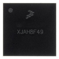
MC13224V Freescale Semiconductor, MC13224V Datasheet - Page 48

MC13224V
Manufacturer Part Number
MC13224V
Description
ZIGBEE PLATFORM 802.15.4 145-LGA
Manufacturer
Freescale Semiconductor
Datasheet
1.1322XUSB.pdf
(54 pages)
Specifications of MC13224V
Frequency
2.4GHz
Data Rate - Maximum
250kbps
Modulation Or Protocol
802.15.4 Zigbee
Applications
General Purpose
Power - Output
4dBm
Sensitivity
-100dBm
Voltage - Supply
2 V ~ 3.6 V
Current - Receiving
24mA
Current - Transmitting
29mA
Data Interface
PCB, Surface Mount
Memory Size
128kB Flash, 96kB RAM
Antenna Connector
PCB, Surface Mount
Operating Temperature
-40°C ~ 105°C
Package / Case
145-LGA
Number Of Receivers
1
Number Of Transmitters
1
Wireless Frequency
2.4 GHz
Interface Type
4-Wire SPI, I2C
Output Power
1.5 dBm
Operating Supply Voltage
2 V to 3.6 V
Maximum Operating Temperature
+ 105 C
Mounting Style
SMD/SMT
Maximum Supply Current
31 mA
Minimum Operating Temperature
- 40 C
Modulation
OQPSK
Protocol Supported
802.15.4
No. Of Pins
99
Supply Voltage Range
2V To 3.6V
Operating Temperature Range
-40°C To +125°C
Msl
MSL 3 - 168 Hours
A/d Converter
12 Bits
No. Of Timers 8/12/16/32 Bits
0 / 0 / 4 / 0
Rohs Compliant
Yes
Lead Free Status / RoHS Status
Lead free / RoHS Compliant
Available stocks
Company
Part Number
Manufacturer
Quantity
Price
Company:
Part Number:
MC13224V
Manufacturer:
Freescale Semiconductor
Quantity:
1 849
Company:
Part Number:
MC13224VR2
Manufacturer:
EPCOS
Quantity:
34 000
8
The MC1322x family is supported by a full set of hardware/software evaluation and development tools.
8.1
The ARM debug environment supports both a JTAG debug interface and an extended capability Nexus
interface.
8.1.1
The JTAG port is the simpler and more common debug port for the ARM core. A standard 20-pin
connector as described in
TMS, TCK, TDO, and RTCK signals of the MC1322x. Through the JTAG serial interface, standard debug
and development activities such as accessing memory and registers, control of the CPU, download of
FLASH memory, and software debug can be accomplished.
8.1.2
The development and debug environment of the ARM7TDMI-S core is based on the A7S Nexus3 interface
(compliant with a Class 3 device of the IEEE-ISTO 5001 standard for real-time embedded system design).
This interface allows expansion of the development features of the JTAG port (through the addition of
auxiliary signals, see
48
1
Resolution
Effective Resolution
Number of input channels
ADC conversion clock frequency
Conversion cycles (continuous convert)
Conversion time
Input Leakage Current
Analog Input Voltage
Analog input must be between V
•
Developer Environment
Program Trace via Branch Trace Messaging (BTM). Branch trace messaging displays program
flow discontinuities (direct and indirect branches, exceptions, etc.), allowing the development tool
to interpolate what transpires between the discontinuities. Thus static code may be traced.
Hardware Development Interfaces
JTAG Hardware Debug Port
A7S Nexus3 (NEX) ARM7 Core Development Interface
Characteristic
1
Section 6.2.2, “Nexus Mictor Interface
Section 6.2.1, “ARM JTAG Interface
Table 23. ADC Timing/Performance Characteristics
REFL
+ 0.2 and V
Symbol
f
ADCCLK
T
MC1322x Technical Data, Rev. 1.3
CCP
V
conv
AIN
REFH
- 0.2 for valid conversion.
Condition
VDD
Connector”). Development features include:
Connector””, is connected to the TDI,
V
Min
REFL
20
—
-
Typ
—
—
8
6
-
-
Freescale Semiconductor
V
Max
300
REFH
12
8
-
-
ADCCLK
cycles
Unit
KHz
Bits
Bits
nA
μs
V


