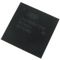
LPC2420FET208,551 NXP Semiconductors, LPC2420FET208,551 Datasheet - Page 44

LPC2420FET208,551
Manufacturer Part Number
LPC2420FET208,551
Description
IC ARM7 MCU 16BIT T208FBGA
Manufacturer
NXP Semiconductors
Series
LPC2400r
Datasheet
1.LPC2460FBD208551.pdf
(79 pages)
Specifications of LPC2420FET208,551
Core Processor
ARM7
Core Size
16/32-Bit
Speed
72MHz
Connectivity
EBI/EMI, I²C, Microwire, MMC, SPI, SSI, SSP, UART/USART, USB OTG
Peripherals
Brown-out Detect/Reset, DMA, I²S, POR, PWM, WDT
Number Of I /o
160
Program Memory Type
ROMless
Ram Size
82K x 8
Voltage - Supply (vcc/vdd)
3 V ~ 3.6 V
Data Converters
A/D 8x10b; D/A 1x10b
Oscillator Type
Internal
Operating Temperature
-40°C ~ 85°C
Package / Case
208-TFBGA
Processor Series
LPC2420
Core
ARM7
Data Bus Width
16 bit, 32 bit
Data Ram Size
98 KB
Interface Type
SPI, I2C, I2S, USB, SSP
Maximum Clock Frequency
72 MHz
Number Of Programmable I/os
160
Number Of Timers
4
Maximum Operating Temperature
+ 85 C
Mounting Style
SMD/SMT
Minimum Operating Temperature
- 40 C
Processor To Be Evaluated
ARM7TDMI-S
Lead Free Status / RoHS Status
Lead free / RoHS Compliant
Program Memory Size
-
Eeprom Size
-
Lead Free Status / Rohs Status
Details
Other names
568-5216
Available stocks
Company
Part Number
Manufacturer
Quantity
Price
Company:
Part Number:
LPC2420FET208,551
Manufacturer:
MAX
Quantity:
65
Company:
Part Number:
LPC2420FET208,551
Manufacturer:
NXP Semiconductors
Quantity:
10 000
NXP Semiconductors
LPC2420_60_5
Preliminary data sheet
7.25.1 Reset
7.25.2 Boot process
7.25.3 Brownout detection
7.25 System control
Reset has four sources on the LPC2420/2460: the RESET pin, the Watchdog reset,
power-on reset, and the BrownOut Detection (BOD) circuit. The RESET pin is a Schmitt
trigger input pin. Assertion of chip Reset by any source, once the operating voltage attains
a usable level, starts the wake-up timer (see description in
timer”), causing reset to remain asserted until the external Reset is de-asserted, the
oscillator is running, and a fixed number of clocks have passed.
Once the internal reset is removed, all of the processor and peripheral registers have
been initialized to predetermined values and the LPC2420/2460 continues with booting
from an external static memory.
The processor always boots from the off-chip static memory bank 1, executing code from
address 0x8100 0000 (see
the boot process initiated by POR, the boot pins P3[15]/D15 and P3[14]/D14 are sampled,
and the external memory banks 0 and 1 are configured with the same data bus width. The
data bus width is determined by the setting of the two boot pins. Unused address pins are
configured as GPIO. See
an example of address and data bus interfacing.
Remark: After POR, the address ranges of chip select 1 and chip select 0 are swapped.
The user code residing in the external boot memory must be linked to execute from
address location 0x8000 0000.
When booting from external memory, the interrupt vectors are mapped to the bottom of
the external memory. Once booting is over, the application must map interrupt vectors to
the proper domain.
The LPC2420/2460 includes 2-stage monitoring of the voltage on the V
If this voltage falls below 2.95 V, the BOD asserts an interrupt signal to the Vectored
Interrupt Controller. This signal can be enabled for interrupt in the Interrupt Enable
Register in the VIC in order to cause a CPU interrupt; if not, software can monitor the
signal by reading a dedicated status register.
The second stage of low-voltage detection asserts a BOD Reset and generates a Reset (if
this reset source is enabled in software) to inactivate the LPC2420/2460 when the voltage
on the V
below 1 V, at which point the power-on reset circuitry maintains the overall Reset.
Both the 2.95 V and 2.65 V thresholds include some hysteresis. In normal operation, this
hysteresis allows the 2.95 V detection to reliably interrupt, or a regularly-executed event
loop to sense the condition.
DD(DCDC)(3V3)
Rev. 05 — 24 February 2010
pins falls below 2.65 V. The BOD circuit maintains this reset down
Section 13.4 “Suggested boot memory interface solutions”
Table 5 “LPC2420/2460 memory usage and
Flashless 16-bit/32-bit microcontroller
Section 7.24.3 “Wake-up
LPC2420/2460
DD(DCDC)(3V3)
© NXP B.V. 2010. All rights reserved.
details”). During
44 of 79
pins.
for


