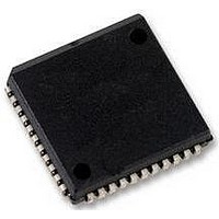
SC16C550BIA44 NXP Semiconductors, SC16C550BIA44 Datasheet - Page 16

SC16C550BIA44
Manufacturer Part Number
SC16C550BIA44
Description
UART, 16BYTE FIFO, 16C550, PLCC44
Manufacturer
NXP Semiconductors
Datasheet
1.SC16C550BIA44518.pdf
(48 pages)
Specifications of SC16C550BIA44
No. Of Channels
1
Data Rate
3Mbps
Supply Voltage Range
2.25V To 5.5V
Operating Temperature Range
-40°C To +85°C
Digital Ic Case Style
PLCC
No. Of Pins
44
Svhc
No SVHC (18-Jun-2010)
Operating
RoHS Compliant
Uart Features
Automatic Hardware Flow Control, Software Selectable Baud Rate Generator
Rohs Compliant
Yes
Available stocks
Company
Part Number
Manufacturer
Quantity
Price
Company:
Part Number:
SC16C550BIA44
Manufacturer:
NXPLIPS
Quantity:
3 000
Part Number:
SC16C550BIA44
Manufacturer:
NXP/恩智浦
Quantity:
20 000
Company:
Part Number:
SC16C550BIA44
Manufacturer:
NXP
Quantity:
15 318
Company:
Part Number:
SC16C550BIA44,512
Manufacturer:
NXP Semiconductors
Quantity:
10 000
Company:
Part Number:
SC16C550BIA44,518
Manufacturer:
NXP Semiconductors
Quantity:
10 000
NXP Semiconductors
SC16C550B_5
Product data sheet
6.7 Loopback mode
The internal loopback capability allows on-board diagnostics. In the loopback mode, the
normal modem interface pins are disconnected and reconfigured for loopback internally.
MCR[3:0] register bits are used for controlling loopback diagnostic testing. In the loopback
mode, OUT1 (bit 2) and OUT2 (bit 3) in the MCR register control the modem RI and DCD
inputs, respectively. MCR signals DTR and RTS (bits 0:1) are used to control the modem
CTS and DSR inputs, respectively. The transmitter output (TX) and the receiver input (RX)
are disconnected from their associated interface pins, and instead are connected together
internally (see
their normal modem control input pins, and instead are connected internally to DTR, RTS,
OUT1 and OUT2. Loopback test data is entered into the transmit holding register via the
user data bus interface, D0 to D7. The transmit UART serializes the data and passes the
serial data to the receive UART via the internal loopback connection. The receive UART
converts the serial data back into parallel data that is then made available at the user data
interface D0 to D7. The user optionally compares the received data to the initial
transmitted data for verifying error-free operation of the UART TX/RX circuits.
In this mode, the receiver and transmitter interrupts are fully operational. The Modem
Control Interrupts are also operational. However, the interrupts can only be read using the
lower four bits of the Modem Status Register (MSR[3:0]) instead of the four Modem Status
Register bits 7:4. The interrupts are still controlled by the IER.
Figure
11). The inputs CTS, DSR, DCD, and RI are disconnected from
Rev. 05 — 1 October 2008
5 V, 3.3 V and 2.5 V UART with 16-byte FIFOs
SC16C550B
© NXP B.V. 2008. All rights reserved.
16 of 48


