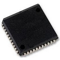
SC16C550BIA44 NXP Semiconductors, SC16C550BIA44 Datasheet - Page 20

SC16C550BIA44
Manufacturer Part Number
SC16C550BIA44
Description
UART, 16BYTE FIFO, 16C550, PLCC44
Manufacturer
NXP Semiconductors
Datasheet
1.SC16C550BIA44518.pdf
(48 pages)
Specifications of SC16C550BIA44
No. Of Channels
1
Data Rate
3Mbps
Supply Voltage Range
2.25V To 5.5V
Operating Temperature Range
-40°C To +85°C
Digital Ic Case Style
PLCC
No. Of Pins
44
Svhc
No SVHC (18-Jun-2010)
Operating
RoHS Compliant
Uart Features
Automatic Hardware Flow Control, Software Selectable Baud Rate Generator
Rohs Compliant
Yes
Available stocks
Company
Part Number
Manufacturer
Quantity
Price
Company:
Part Number:
SC16C550BIA44
Manufacturer:
NXPLIPS
Quantity:
3 000
Part Number:
SC16C550BIA44
Manufacturer:
NXP/恩智浦
Quantity:
20 000
Company:
Part Number:
SC16C550BIA44
Manufacturer:
NXP
Quantity:
15 318
Company:
Part Number:
SC16C550BIA44,512
Manufacturer:
NXP Semiconductors
Quantity:
10 000
Company:
Part Number:
SC16C550BIA44,518
Manufacturer:
NXP Semiconductors
Quantity:
10 000
NXP Semiconductors
SC16C550B_5
Product data sheet
7.3.1.1 Mode 0 (FCR bit 3 = 0)
7.3.1.2 Mode 1 (FCR bit 3 = 1)
7.2.1 IER versus Receive FIFO interrupt mode operation
7.2.2 IER versus Receive/Transmit FIFO polled mode operation
7.3.1 DMA mode
7.3 FIFO Control Register (FCR)
When the receive FIFO (FCR[0] = logic 1), and receive interrupts (IER[0] = logic 1) are
enabled, the receive interrupts and register status will reflect the following:
When FCR[0] = logic 1, resetting IER[0:3] enables the SC16C550B in the FIFO polled
mode of operation. Since the receiver and transmitter have separate bits in the LSR,
either or both can be used in the polled mode by selecting respective transmit or receive
control bit(s).
This register is used to enable the FIFOs, clear the FIFOs, set the receive FIFO trigger
levels, and select the DMA mode.
(DMA mode does not exist in the HVQFN32 package; see
Set and enable the interrupt for each single transmit or receive operation, and is similar to
the 16C450 mode. Transmit Ready (TXRDY) will go to a logic 0 whenever an empty
transmit space is available in the Transmit Holding Register (THR). Receive Ready
(RXRDY) will go to a logic 0 whenever the Receive Holding Register (RHR) is loaded with
a character.
Set and enable the interrupt in a block mode operation. The transmit interrupt is set when
the transmit FIFO is empty. The receive interrupt is set when the receive FIFO fills to the
programmed trigger level. However, the FIFO continues to fill regardless of the
programmed level until the FIFO is full. RXRDY remains a logic 0 as long as the FIFO fill
level is above the programmed trigger level.
•
•
•
•
•
•
•
•
The receive data available interrupts are issued to the external CPU when the FIFO
has reached the programmed trigger level. It will be cleared when the FIFO drops
below the programmed trigger level.
FIFO status will also be reflected in the user accessible ISR register when the FIFO
trigger level is reached. Both the ISR register status bit and the interrupt will be
cleared when the FIFO drops below the trigger level.
The data ready bit (LSR[0]) is set as soon as a character is transferred from the shift
register to the receive FIFO. It is reset when the FIFO is empty.
LSR[0] will be a logic 1 as long as there is one byte in the receive FIFO.
LSR[1:4] will provide the type of errors encountered, if any.
LSR[5] will indicate when the transmit FIFO is empty.
LSR[6] will indicate when both the transmit FIFO and transmit shift register are empty.
LSR[7] will indicate any FIFO data errors.
Rev. 05 — 1 October 2008
5 V, 3.3 V and 2.5 V UART with 16-byte FIFOs
Table
SC16C550B
9.)
© NXP B.V. 2008. All rights reserved.
20 of 48


