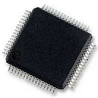
SC16C750BIB64 NXP Semiconductors, SC16C750BIB64 Datasheet - Page 13

SC16C750BIB64
Manufacturer Part Number
SC16C750BIB64
Description
UART, 64BYTE FIFO, 16C750, LQFP64
Manufacturer
NXP Semiconductors
Datasheet
1.SC16C750BIA44518.pdf
(44 pages)
Specifications of SC16C750BIB64
No. Of Channels
1
Data Rate
3Mbps
Supply Voltage Range
2.25V To 5.5V
Operating Temperature Range
-40°C To +85°C
Digital Ic Case Style
LQFP
No. Of Pins
64
Svhc
No SVHC (18-Jun-2010)
Operating
RoHS Compliant
Uart Features
Automatic Hardware Flow Control, Software Selectable Baud Rate Generator
Rohs Compliant
Yes
Available stocks
Company
Part Number
Manufacturer
Quantity
Price
Company:
Part Number:
SC16C750BIB64,128
Manufacturer:
NXP Semiconductors
Quantity:
10 000
Company:
Part Number:
SC16C750BIB64,151
Manufacturer:
NXP Semiconductors
Quantity:
10 000
Company:
Part Number:
SC16C750BIB64,157
Manufacturer:
NXP Semiconductors
Quantity:
10 000
Company:
Part Number:
SC16C750BIB64157
Manufacturer:
NXP Semiconductors
Quantity:
135
NXP Semiconductors
SC16C750B_5
Product data sheet
6.7 Sleep mode
6.8 Low power mode
6.9 Loopback mode
The SC16C750B is designed to operate with low power consumption. A special Sleep
mode is included to further reduce power consumption (the internal oscillator driver is
disabled) when the chip is not being used. With IER[4] enabled (set to a logic 1), the
SC16C750B enters the Sleep mode, but resumes normal operation when a start bit is
detected, a change of state of RX or on any of the modem input pins RI, CTS, DSR, DCD,
or a transmit data is provided by the user. If the Sleep mode is enabled and the
SC16C750B is awakened by one of the conditions described above, it will return to the
Sleep mode automatically after the last character is transmitted or read by the user. In any
case, the Sleep mode will not be entered while an interrupt(s) is pending. The
SC16C750B will stay in the Sleep mode of operation until it is disabled by setting IER[4] to
a logic 0.
In Low power mode the oscillator is still running and only the clock to the UART core is
cut off. This helps to reduce the operating current to about
the same conditions as in Sleep mode.
The internal loopback capability allows on-board diagnostics. In the Loopback mode, the
normal modem interface pins are disconnected and reconfigured for loopback internally.
MCR[3:0] register bits are used for controlling loopback diagnostic testing. In the
Loopback mode, OUT1 and OUT2 in the MCR register (bit 2 and bit 3) control the modem
RI and DCD inputs, respectively. MCR signals DTR and RTS (bit 0 and bit 1) are used to
control the modem DSR and CTS inputs, respectively. The transmitter output (TX) and the
receiver input (RX) are disconnected from their associated interface pins, and instead are
connected together internally (see
disconnected from their normal modem control input pins, and instead are connected
internally to RTS, DTR, OUT2 and OUT1. Loopback test data is entered into the Transmit
Holding Register via the user data bus interface, D0 to D7. The transmit UART serializes
the data and passes the serial data to the receive UART via the internal loopback
connection. The receive UART converts the serial data back into parallel data that is then
made available at the user data interface D0 to D7. The user optionally compares the
received data to the initial transmitted data for verifying error-free operation of the UART
TX/RX circuits.
Rev. 05 — 17 October 2008
Figure
5 V, 3.3 V and 2.5 V UART with 64-byte FIFOs
6). The CTS, DSR, DCD, and RI are
1
3
. The UART wakes up under
SC16C750B
© NXP B.V. 2008. All rights reserved.
13 of 44


