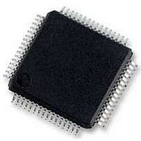
SC16C750BIB64 NXP Semiconductors, SC16C750BIB64 Datasheet - Page 23

SC16C750BIB64
Manufacturer Part Number
SC16C750BIB64
Description
UART, 64BYTE FIFO, 16C750, LQFP64
Manufacturer
NXP Semiconductors
Datasheet
1.SC16C750BIA44518.pdf
(44 pages)
Specifications of SC16C750BIB64
No. Of Channels
1
Data Rate
3Mbps
Supply Voltage Range
2.25V To 5.5V
Operating Temperature Range
-40°C To +85°C
Digital Ic Case Style
LQFP
No. Of Pins
64
Svhc
No SVHC (18-Jun-2010)
Operating
RoHS Compliant
Uart Features
Automatic Hardware Flow Control, Software Selectable Baud Rate Generator
Rohs Compliant
Yes
Available stocks
Company
Part Number
Manufacturer
Quantity
Price
Company:
Part Number:
SC16C750BIB64,128
Manufacturer:
NXP Semiconductors
Quantity:
10 000
Company:
Part Number:
SC16C750BIB64,151
Manufacturer:
NXP Semiconductors
Quantity:
10 000
Company:
Part Number:
SC16C750BIB64,157
Manufacturer:
NXP Semiconductors
Quantity:
10 000
Company:
Part Number:
SC16C750BIB64157
Manufacturer:
NXP Semiconductors
Quantity:
135
NXP Semiconductors
SC16C750B_5
Product data sheet
7.6 Modem Control Register (MCR)
This register controls the interface with the modem or a peripheral device.
Table 18.
The flow control can be configured by programming MCR[1] and MCR[5] as shown in
Table
Table 19.
Bit
7
6
5
4
3
2
1
0
MCR[5] (AFE)
1
1
0
19.
Symbol
MCR[7]
MCR[6]
MCR[5]
MCR[4]
MCR[3]
MCR[2]
MCR[1]
MCR[0]
Modem Control Register bits description
Flow control configuration
Description
reserved; set to 0
reserved; set to 0
AFE. This bit is the auto flow control enable. When this bit is set, the auto
flow control is enabled.
Loopback. Enable the local Loopback mode (diagnostics). In this mode the
transmitter output (TX) and the receiver input (RX), CTS, DSR, DCD, and RI
are disconnected from the SC16C750B I/O pins. Internally the modem data
and control pins are connected into a loopback data configuration (see
Figure
operational. The Modem Control Interrupts are also operational, but the
interrupts’ sources are switched to the lower four bits of the Modem Control.
Interrupts continue to be controlled by the IER register.
OUT2, INT enable. Used to control the modem DCD signal in the Loopback
mode.
OUT1. This bit is used in the Loopback mode only. In the Loopback mode,
this bit is used to write the state of the modem RI interface signal via OUT1.
RTS
DTR
Rev. 05 — 17 October 2008
logic 0 = disable Loopback mode (normal default condition)
logic 1 = enable local Loopback mode (diagnostics)
logic 0 = set OUT2 to HIGH. In the Loopback mode, sets OUT2 (DCD)
internally to a logic 1.
logic 1 = set OUT2 to LOW. In the Loopback mode, sets OUT2 (DCD)
internally to a logic 0.
logic 0 = force RTS output to a logic 1 (normal default condition)
logic 1 = force RTS output to a logic 0
logic 0 = force DTR output to a logic 1 (normal default condition)
logic 1 = force DTR output to a logic 0
MCR[1] (RTS)
1
0
X
6). In this mode, the receiver and transmitter interrupts remain fully
5 V, 3.3 V and 2.5 V UART with 64-byte FIFOs
Flow configuration
auto RTS and CTS enabled
auto CTS only enabled
auto RTS and CTS disabled
SC16C750B
© NXP B.V. 2008. All rights reserved.
23 of 44


