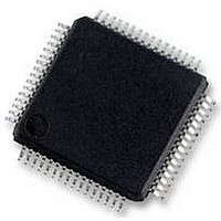
SC16C750BIB64 NXP Semiconductors, SC16C750BIB64 Datasheet - Page 17

SC16C750BIB64
Manufacturer Part Number
SC16C750BIB64
Description
UART, 64BYTE FIFO, 16C750, LQFP64
Manufacturer
NXP Semiconductors
Datasheet
1.SC16C750BIA44518.pdf
(44 pages)
Specifications of SC16C750BIB64
No. Of Channels
1
Data Rate
3Mbps
Supply Voltage Range
2.25V To 5.5V
Operating Temperature Range
-40°C To +85°C
Digital Ic Case Style
LQFP
No. Of Pins
64
Svhc
No SVHC (18-Jun-2010)
Operating
RoHS Compliant
Uart Features
Automatic Hardware Flow Control, Software Selectable Baud Rate Generator
Rohs Compliant
Yes
Available stocks
Company
Part Number
Manufacturer
Quantity
Price
Company:
Part Number:
SC16C750BIB64,128
Manufacturer:
NXP Semiconductors
Quantity:
10 000
Company:
Part Number:
SC16C750BIB64,151
Manufacturer:
NXP Semiconductors
Quantity:
10 000
Company:
Part Number:
SC16C750BIB64,157
Manufacturer:
NXP Semiconductors
Quantity:
10 000
Company:
Part Number:
SC16C750BIB64157
Manufacturer:
NXP Semiconductors
Quantity:
135
NXP Semiconductors
SC16C750B_5
Product data sheet
7.2.1 IER versus Receive FIFO interrupt mode operation
7.2.2 IER versus Receive/Transmit FIFO polled mode operation
Table 9.
When the receive FIFO (FCR[0] = logic 1), and receive interrupts (IER[0] = logic 1) are
enabled, the receive interrupts and register status will reflect the following:
When FCR[0] = logic 1, resetting IER[3:0] enables the SC16C750B in the FIFO polled
mode of operation. Since the receiver and transmitter have separate bits in the LSR,
either or both can be used in the polled mode by selecting respective transmit or receive
control bit(s).
Bit
1
0
•
•
•
•
•
•
•
•
The receive data available interrupts are issued to the external CPU when the FIFO
has reached the programmed trigger level. It will be cleared when the FIFO drops
below the programmed trigger level.
FIFO status will also be reflected in the user accessible ISR register when the FIFO
trigger level is reached. Both the ISR register status bit and the interrupt will be
cleared when the FIFO drops below the trigger level.
The data ready bit (LSR[0]) is set as soon as a character is transferred from the shift
register to the receive FIFO. It is reset when the FIFO is empty.
LSR[0] will be a logic 1 as long as there is one byte in the receive FIFO.
LSR[4:1] will provide the type of errors encountered, if any.
LSR[5] will indicate when the transmit FIFO is empty.
LSR[6] will indicate when both the transmit FIFO and transmit shift register are empty.
LSR[7] will indicate any FIFO data errors.
Symbol
IER[1]
IER[0]
Interrupt Enable Register bits description
Description
Transmit Holding Register interrupt. This interrupt will be issued whenever the
THR is empty, and is associated with LSR[1].
Receive Holding Register interrupt. This interrupt will be issued when the FIFO
has reached the programmed trigger level, or is cleared when the FIFO drops
below the trigger level in the FIFO mode of operation.
logic 0 = disable the transmitter empty interrupt (normal default condition)
logic 1 = enable the transmitter empty interrupt
logic 0 = disable the receiver ready interrupt (normal default condition)
logic 1 = enable the receiver ready interrupt
Rev. 05 — 17 October 2008
5 V, 3.3 V and 2.5 V UART with 64-byte FIFOs
…continued
SC16C750B
© NXP B.V. 2008. All rights reserved.
17 of 44


