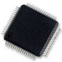
SC16C750BIB64 NXP Semiconductors, SC16C750BIB64 Datasheet - Page 19

SC16C750BIB64
Manufacturer Part Number
SC16C750BIB64
Description
UART, 64BYTE FIFO, 16C750, LQFP64
Manufacturer
NXP Semiconductors
Datasheet
1.SC16C750BIA44518.pdf
(44 pages)
Specifications of SC16C750BIB64
No. Of Channels
1
Data Rate
3Mbps
Supply Voltage Range
2.25V To 5.5V
Operating Temperature Range
-40°C To +85°C
Digital Ic Case Style
LQFP
No. Of Pins
64
Svhc
No SVHC (18-Jun-2010)
Operating
RoHS Compliant
Uart Features
Automatic Hardware Flow Control, Software Selectable Baud Rate Generator
Rohs Compliant
Yes
Available stocks
Company
Part Number
Manufacturer
Quantity
Price
Company:
Part Number:
SC16C750BIB64,128
Manufacturer:
NXP Semiconductors
Quantity:
10 000
Company:
Part Number:
SC16C750BIB64,151
Manufacturer:
NXP Semiconductors
Quantity:
10 000
Company:
Part Number:
SC16C750BIB64,157
Manufacturer:
NXP Semiconductors
Quantity:
10 000
Company:
Part Number:
SC16C750BIB64157
Manufacturer:
NXP Semiconductors
Quantity:
135
NXP Semiconductors
SC16C750B_5
Product data sheet
Table 10.
Table 11.
Bit
2
1
0
FCR[7]
0
0
1
1
Symbol
FCR[3]
(continued)
FCR[2]
FCR[1]
FCR[0]
FIFO Control Register bits description
RCVR trigger levels
FCR[6]
0
1
0
1
Description
Transmit operation in mode ‘1’: When the SC16C750B is in FIFO mode
(FCR[0] = logic 1; FCR[3] = logic 1), the TXRDY pin will be a logic 1 when
the transmit FIFO is completely full. It will be a logic 0 when the FIFO is
emptied.
Receive operation in mode ‘1’: When the SC16C750B is in FIFO mode
(FCR[0] = logic 1; FCR[3] = logic 1) and the trigger level has been reached,
or a Receive Time-Out has occurred, the RXRDY pin will go to a logic 0.
Once activated, it will go to a logic 1 after there are no more characters in
the FIFO.
XMIT FIFO reset.
RCVR FIFO reset.
FIFO enable.
Rev. 05 — 17 October 2008
logic 0 = no FIFO transmit reset (normal default condition)
logic 1 = clears the contents of the transmit FIFO and resets the FIFO
counter logic (the transmit shift register is not cleared or altered). This bit
will return to a logic 0 after clearing the FIFO.
logic 0 = no FIFO receive reset (normal default condition)
logic 1 = clears the contents of the receive FIFO and resets the FIFO
counter logic (the receive shift register is not cleared or altered). This bit
will return to a logic 0 after clearing the FIFO.
logic 0 = disable the transmit and receive FIFO (normal default condition)
logic 1 = enable the transmit and receive FIFO
RX FIFO trigger level (bytes)
16-byte operation
1
4
8
14
5 V, 3.3 V and 2.5 V UART with 64-byte FIFOs
…continued
64-byte operation
1
16
32
56
SC16C750B
© NXP B.V. 2008. All rights reserved.
19 of 44


