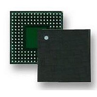
LH7A404N0F000B3 NXP Semiconductors, LH7A404N0F000B3 Datasheet - Page 19

LH7A404N0F000B3
Manufacturer Part Number
LH7A404N0F000B3
Description
MCU ARM9, LCD CTRL, SMD, LFBGA-324
Manufacturer
NXP Semiconductors
Datasheet
1.LH7A404N0F000B3.pdf
(75 pages)
Specifications of LH7A404N0F000B3
Core Size
32bit
No. Of I/o's
64
Ram Memory Size
80KB
Cpu Speed
200MHz
Oscillator Type
External Only
No. Of Timers
3
No. Of Pwm Channels
4
Digital Ic Case Style
LFBGA
Supply Voltage Range
3V
Controller Family/series
LH7A
Peripherals
ADC, DMA, RTC
Rohs Compliant
Yes
Data Bus Width
32 bit
Program Memory Type
ROMLess
Data Ram Size
80 KB
Interface Type
EBI , IrDA , JTAG , PS2 , SCI , UART , USB
Maximum Clock Frequency
200 MHz
Number Of Programmable I/os
64
Number Of Timers
3
Maximum Operating Temperature
+ 85 C
Mounting Style
SMD/SMT
Package / Case
LFBGA
Minimum Operating Temperature
- 40 C
On-chip Adc
10 bit, 9 Channel
Lead Free Status / RoHS Status
Lead free / RoHS Compliant
Available stocks
Company
Part Number
Manufacturer
Quantity
Price
Company:
Part Number:
LH7A404N0F000B3
Manufacturer:
AD
Quantity:
5 742
Company:
Part Number:
LH7A404N0F000B3,55
Manufacturer:
NXP Semiconductors
Quantity:
10 000
32-Bit System-on-Chip
Power Modes
Halt, and Standby. During Run all clocks are hardware
enabled and the processor is clocked. In the Halt mode
the device is functioning, but the processor clock is
halted while it waits for an event such as a key press.
Standby equates to the computer being switched ‘off’,
i.e. no display (LCD disabled) and the main oscillator is
shut down.
Reset Modes
LH7A404: nPOR (power on reset), nPWRFL (power
failure) and nURESET (user reset). If any of these are
active, a system reset is internally generated. An nPOR
reset performs a full system reset. The nPWRFL and
nURESET resets perform a full system reset except for
the SDRAM refresh control, SDRAM Global Configura-
tion, SDRAM Device Configuration, and the RTC
peripheral registers. The SDRAM controller issues a
self-refresh command to external SDRAM before the
system enters an nPWRFL and nURESET reset. This
allows the system to maintain its Real Time Clock and
SDRAM contents. Upon release of Reset, the chip
enters Standby mode. Once in the Run mode the
PWRSR register can be interrogated to determine the
nature of the reset and the trigger source, after which
software can then take appropriate actions.
Preliminary data sheet
The LH7A404 has three operational states: Run,
Three external signals can generate resets to the
14.7456 MHz
32.768 kHz
RTC OSC
ƒIN
PLL1
DIVIDE BY
PREDIV+2
DIVIDE BY MAINDIV1+2
MAIN DIVIDER 1:
Figure 3. Clock and State Controller Block Diagram
500 kHz
MIN.
VCO
80 and 400 MHz
DIVIDE BY MAINDIV2+2
BETWEEN
MUST BE
NXP Semiconductors
MAIN DIVIDER 2:
DIVIDE
BY 2
Data Paths
• The AMBA AHB bus
• The AMBA APB bus
• The External Bus Interface
• The LCD AHB bus
• The DMA busses.
AMBA AHB BUS
AHB (AMBA AHB) is a high speed 32-bit-wide data bus.
The AMBA AHB is for high-performance, high-clock-fre-
quency system modules.
width requirements are connected to the ARM922T
processor and other bus masters using a multi-master
AHB bus. These peripherals include the external mem-
ory interfaces, on-chip SRAM, LCD Controller (bus
master), DMA Controller (bus master), and USB Host
(bus master). Remaining peripherals reside on the
lower bandwidth Advanced Peripheral Bus (APB),
which is accessed from the AHB via the APB Bridge.
The APB Bridge is the only master on the APB, and its
operation is transparent to the user as it converts AHB
accesses into slower APB accesses automatically.
PS
The data paths in the LH7A404 are:
The Advanced Microprocessor Bus Architecture
LH7A404 peripherals and memory with high band-
GCLK
RTC
32.768 kHz
HCLKDIV
GATE
PCLKDIV
GATE
FCLK
HCLK_CPU
HCLK
PCLK
LH7A404-6
LH7A404
19


