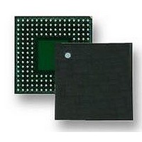
LH7A404N0F000B3 NXP Semiconductors, LH7A404N0F000B3 Datasheet - Page 23

LH7A404N0F000B3
Manufacturer Part Number
LH7A404N0F000B3
Description
MCU ARM9, LCD CTRL, SMD, LFBGA-324
Manufacturer
NXP Semiconductors
Datasheet
1.LH7A404N0F000B3.pdf
(75 pages)
Specifications of LH7A404N0F000B3
Core Size
32bit
No. Of I/o's
64
Ram Memory Size
80KB
Cpu Speed
200MHz
Oscillator Type
External Only
No. Of Timers
3
No. Of Pwm Channels
4
Digital Ic Case Style
LFBGA
Supply Voltage Range
3V
Controller Family/series
LH7A
Peripherals
ADC, DMA, RTC
Rohs Compliant
Yes
Data Bus Width
32 bit
Program Memory Type
ROMLess
Data Ram Size
80 KB
Interface Type
EBI , IrDA , JTAG , PS2 , SCI , UART , USB
Maximum Clock Frequency
200 MHz
Number Of Programmable I/os
64
Number Of Timers
3
Maximum Operating Temperature
+ 85 C
Mounting Style
SMD/SMT
Package / Case
LFBGA
Minimum Operating Temperature
- 40 C
On-chip Adc
10 bit, 9 Channel
Lead Free Status / RoHS Status
Lead free / RoHS Compliant
Available stocks
Company
Part Number
Manufacturer
Quantity
Price
Company:
Part Number:
LH7A404N0F000B3
Manufacturer:
AD
Quantity:
5 742
Company:
Part Number:
LH7A404N0F000B3,55
Manufacturer:
NXP Semiconductors
Quantity:
10 000
32-Bit System-on-Chip
Embedded SRAM
SRAM. This embedded memory is used for storing
code, data, or LCD frame data and is contiguous with
external SDRAM. The 80 kB is large enough to store a
QVGA frame (320 × 240) at 8 bits per pixel, equivalent
to 70 kB of information.
power consumed by LH7A404 applications. Normally,
the system performs external accesses to acquire this
data. The LCD controller automatically uses an over-
flow frame buffer in SDRAM if a larger screen size is
required. This overflow buffer can be located on any
4 kB page boundary in SDRAM, allowing software to
set the MMU (in the LCD controller) page tables so the
two memory areas appear contiguous, allowing byte,
half-word, and word accesses.
Static Memory Controller (SMC)
provides an interface between the AMBA AHB system
bus and external (off-chip) memory devices.
pendently configurable memory banks. Each memory
bank can support:
• SRAM
• ROM
• Flash EPROM
• Burst ROM memory.
8-, 16-, or 32-bit external memory data paths. The
memory controller is configured to support little-endian
operation only.
• Non-burst read and write accesses only to high-
• Non-burst write accesses, nonburst read accesses
• Memory bank select
• Access sequencing
• Wait state generation
• Byte lane write control
• External bus interface
• CompactFlash or PCMCIA interfacing.
Preliminary data sheet
speed CMOS static RAM
and asynchronous page mode read accesses to
fast-boot block flash memory.
The LH7A404 incorporates 80 kB of embedded
Locating the frame buffer on chip reduces the overall
The asynchronous Static Memory Controller (SMC)
The SMC simultaneously supports up to eight inde-
Each memory bank may use devices with either
The memory banks can be configured to support:
The SMC has six main functions:
NXP Semiconductors
SDRAM (Synchronous) Memory Controller
vides a high speed memory interface to a wide variety of
synchronous memory devices, including Synchronous
DRAM, Synchronous Flash and Synchronous ROMs.
• LCD DMA port for high bandwidth
• Up to four Synchronous Memory banks can be inde-
• Includes special configuration bits for Synchronous
• Includes ability to program Synchronous Flash
• On booting from Synchronous ROM, (and optionally
• Data is transferred between the controller and the
• Programmable for 16- or 32-bit data bus size
• Two reset domains enable Synchronous DRAM con-
• Power saving Synchronous Memory SCKE and
Secure Digital/MultiMediaCard (MMC)
that meets the security, capacity, performance,
and environment requirements inherent in electronic
devices. The SD Memory Card host supports
MultiMediaCard (MMC) operation as well, and is com-
patible with MMC Cards.
card controller or as an SD Card controller, and sup-
ports the full SD/MMC bus protocol as defined in the
MMC system specification 2.11 provided by the MMC
Association and the ‘SD Memory Card Spec v1.0’ from
the SD Association.
pendently set up
ROM operation
devices using write and erase commands
with Synchronous Flash), a configuration sequence is
performed before releasing the processor from reset
Synchronous DRAM in four-word bursts. Longer
transfers within the same page are concatenated,
forming a seamless burst
tents to be preserved over a ‘soft’ reset
external clock modes provided.
The SDRAM (Synchronous) Memory Controller pro-
The key features of the controller are:
The SD Memory Card is a flash-based memory card
The SD/MMC controller can be used as an MMC
LH7A404
23


