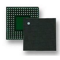
LH7A404N0F000B3 NXP Semiconductors, LH7A404N0F000B3 Datasheet - Page 52

LH7A404N0F000B3
Manufacturer Part Number
LH7A404N0F000B3
Description
MCU ARM9, LCD CTRL, SMD, LFBGA-324
Manufacturer
NXP Semiconductors
Datasheet
1.LH7A404N0F000B3.pdf
(75 pages)
Specifications of LH7A404N0F000B3
Core Size
32bit
No. Of I/o's
64
Ram Memory Size
80KB
Cpu Speed
200MHz
Oscillator Type
External Only
No. Of Timers
3
No. Of Pwm Channels
4
Digital Ic Case Style
LFBGA
Supply Voltage Range
3V
Controller Family/series
LH7A
Peripherals
ADC, DMA, RTC
Rohs Compliant
Yes
Data Bus Width
32 bit
Program Memory Type
ROMLess
Data Ram Size
80 KB
Interface Type
EBI , IrDA , JTAG , PS2 , SCI , UART , USB
Maximum Clock Frequency
200 MHz
Number Of Programmable I/os
64
Number Of Timers
3
Maximum Operating Temperature
+ 85 C
Mounting Style
SMD/SMT
Package / Case
LFBGA
Minimum Operating Temperature
- 40 C
On-chip Adc
10 bit, 9 Channel
Lead Free Status / RoHS Status
Lead free / RoHS Compliant
Available stocks
Company
Part Number
Manufacturer
Quantity
Price
Company:
Part Number:
LH7A404N0F000B3
Manufacturer:
AD
Quantity:
5 742
Company:
Part Number:
LH7A404N0F000B3,55
Manufacturer:
NXP Semiconductors
Quantity:
10 000
LH7A404
the serial frame pin (SSPFRM) is active LOW. Both the
SSP and external slave device drive their output data
on the falling edge of the clock, and latch data from the
other device on the rising edge of the clock. Unlike the
full-duplex transmission of the other two frame formats,
the National Semiconductor MICROWIRE format uti-
lizes a master-slave messaging technique that oper-
ates in half-duplex. When a frame begins in this mode,
52
For National Semiconductor MICROWIRE format,
nSSPFRM
nSSPFRM
SSPRXD
SSPTXD
SSPRXD
SSPCLK
SSPTXD
SSPCLK
LSB
MSB
Figure 31. MICROWIRE Frame Format (Continuous Transfers)
0
Figure 30. MICROWIRE Frame Format (Single Transfer)
MSB
8-BIT CONTROL
OUTPUT DATA
4 to 16 BITS
LSB
NXP Semiconductors
MSB
LSB
0
8-BIT CONTROL
MSB
an 8-bit control message is transmitted to the off-chip
slave. During this transmission no incoming data is
received by the SSP. After the message has been sent,
the external slave device decodes the message. After
waiting one serial clock period after the last bit of the 8-
bit control message was received it responds by return-
ing the requested data. The returned data can be 4 to
16 bits in length, making the total frame length between
13 to 25 bits. See Figure 30 and Figure 31.
OUTPUT DATA
4 to 16 BITS
LSB
LSB
MSB
32-Bit System-on-Chip
Preliminary data sheet
LH7A404-34
LH7A404-35


