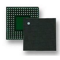
LH7A404N0F000B3 NXP Semiconductors, LH7A404N0F000B3 Datasheet - Page 27

LH7A404N0F000B3
Manufacturer Part Number
LH7A404N0F000B3
Description
MCU ARM9, LCD CTRL, SMD, LFBGA-324
Manufacturer
NXP Semiconductors
Datasheet
1.LH7A404N0F000B3.pdf
(75 pages)
Specifications of LH7A404N0F000B3
Core Size
32bit
No. Of I/o's
64
Ram Memory Size
80KB
Cpu Speed
200MHz
Oscillator Type
External Only
No. Of Timers
3
No. Of Pwm Channels
4
Digital Ic Case Style
LFBGA
Supply Voltage Range
3V
Controller Family/series
LH7A
Peripherals
ADC, DMA, RTC
Rohs Compliant
Yes
Data Bus Width
32 bit
Program Memory Type
ROMLess
Data Ram Size
80 KB
Interface Type
EBI , IrDA , JTAG , PS2 , SCI , UART , USB
Maximum Clock Frequency
200 MHz
Number Of Programmable I/os
64
Number Of Timers
3
Maximum Operating Temperature
+ 85 C
Mounting Style
SMD/SMT
Package / Case
LFBGA
Minimum Operating Temperature
- 40 C
On-chip Adc
10 bit, 9 Channel
Lead Free Status / RoHS Status
Lead free / RoHS Compliant
Available stocks
Company
Part Number
Manufacturer
Quantity
Price
Company:
Part Number:
LH7A404N0F000B3
Manufacturer:
AD
Quantity:
5 742
Company:
Part Number:
LH7A404N0F000B3,55
Manufacturer:
NXP Semiconductors
Quantity:
10 000
32-Bit System-on-Chip
UART/IrDA
UART2, and UART3.
• Serial-to-Parallel conversion on data received from
• Parallel-to-Serial conversion on data transmitted to
through the DMA separately or simultaneously, and are
buffered with internal FIFO memories. This allows up to
16 bytes to be stored independently in both transmit and
receive modes. The UART can generate:
• Four individually maskable interrupts from the
• A single combined interrupt so that the output is
reception, the appropriate error bit is set and stored in
the FIFO. If an overrun condition occurs, the overrun
register bit is set immediately and the FIFO data is pre-
vented from being overwritten. UART1 also supports
IrDA 1.0 (15.2 kbit/s).
(CTS), Data Carrier Detect (DCD) and Data Set Ready
(DSR) are supported on UART2 and UART3.
Timers
Each of the timers can operate in two modes: free run-
ning and pre-scale. The timers are programmed using
four registers; Load, Value, Control, and Clear.
(TC2), use clock sources of either 508 kHz or 2 kHz. The
clock source and mode are selectable by writing to the
appropriate bits in the system control register. Each
timer has a 16-bit read/write data register and a control
register. The timer is immediately loaded with the value
written to the data register. This value is then decre-
mented on the next active clock edge to arrive after the
write. When the timer underflows, it immediately asserts
its appropriate interrupt.
clocked from a single 7.3728 MHz source. Once the
timer has been enabled and written to, it decrements
on the next rising edge of the 7.3728 MHz clock after
the data register has been updated.
Preliminary data sheet
the peripheral device
the peripheral device.
receive, transmit, and modem status logic blocks
asserted if any of the individual interrupts are
asserted and unmasked.
The LH7A404 contains three UARTs; UART1,
The UART performs:
The transmit and receive paths can both be routed
If a framing, parity or break error occurs during
The modem status input signals Clear to Send
The LH7A404 includes three programmable timers.
Two identical timers, Timer 1 (TC1) and Timer 2
Timer 3 (TC3) has the same basic operation, but is
NXP Semiconductors
FREE-RUNNING MODE
0xFFFF when it underflows and continues counting down.
PRE-SCALE MODE
each timer is automatically re-loaded when the timer
underflows. This mode can be used to produce a pro-
grammable frequency to drive the buzzer or generate a
periodic interrupt.
Real Time Clock (RTC)
time-base counter. This is achieved by generating an
interrupt signal after counting for a programmed num-
ber of cycles of a real-time clock input. Counting in one-
second intervals is achieved by use of a 1 Hz clock
input to the RTC.
Keyboard and Mouse Interface (KMI)
following features:
• IBM PS/2 or AT-compatible keyboard or mouse
• Half-duplex, bidirectional synchronous serial inter-
• Programmable 4-bit reference clock divider
• Polled or interrupt-driven mode
• Separately maskable transmit and receive interrupts
• Single combined interrupt output
• Odd parity generation and checking
• Register bits for override of keyboard clock and
for functional verification and manufacturing test.
A/D Converter with Brownout Detector and
Touch Screen Controller
integrated Touch Screen Controller (TSC) and brown-
out detector. The TSC is a complete interface to a
Touch Screen for portable personal devices. It com-
bines the front-end biasing and control circuitry with
A/D conversion, reference generation, and digital inter-
face functions to completely replace external ICs used
to implement this interface. The ADC features:
• A 10-bit A/D converter with integrated sample-and-
• Active matrix for bias and control circuits necessary
interface
face using open-drain outputs for clock and data.
data lines.
hold, fully differential, high impedance signal and ref-
erence inputs
for connection to external 4-, 5-, 7-, and 8-wire touch
panels, including pen pressure implementation
In free-running mode, the timer wraps around to
In pre-scale (periodic) mode, the value written to
The RTC provides a basic alarm function or long
The Keyboard and Mouse Interface has the
Additional test registers and modes are implemented
The LH7A404 includes an A/D Converter (ADC) with
LH7A404
27


