LH7A404N0F000B3 NXP Semiconductors, LH7A404N0F000B3 Datasheet - Page 4
LH7A404N0F000B3
Manufacturer Part Number
LH7A404N0F000B3
Description
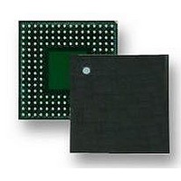
MCU ARM9, LCD CTRL, SMD, LFBGA-324
Manufacturer
NXP Semiconductors
Datasheet
1.LH7A404N0F000B3.pdf
(75 pages)
Specifications of LH7A404N0F000B3
Core Size
32bit
No. Of I/o's
64
Ram Memory Size
80KB
Cpu Speed
200MHz
Oscillator Type
External Only
No. Of Timers
3
No. Of Pwm Channels
4
Digital Ic Case Style
LFBGA
Supply Voltage Range
3V
Controller Family/series
LH7A
Peripherals
ADC, DMA, RTC
Rohs Compliant
Yes
Data Bus Width
32 bit
Program Memory Type
ROMLess
Data Ram Size
80 KB
Interface Type
EBI , IrDA , JTAG , PS2 , SCI , UART , USB
Maximum Clock Frequency
200 MHz
Number Of Programmable I/os
64
Number Of Timers
3
Maximum Operating Temperature
+ 85 C
Mounting Style
SMD/SMT
Package / Case
LFBGA
Minimum Operating Temperature
- 40 C
On-chip Adc
10 bit, 9 Channel
Lead Free Status / RoHS Status
Lead free / RoHS Compliant
Available stocks
Company
Part Number
Manufacturer
Quantity
Price
Company:

Part Number:
LH7A404N0F000B3
Manufacturer:
AD
Quantity:
5 742
Company:
Part Number:
LH7A404N0F000B3,55
Manufacturer:
NXP Semiconductors
Quantity:
10 000


LH7A404
4
LFBGA
W17
W16
W13
R16
U15
E15
F16
T15
Y17
V16
V13
Y18
Y19
T19
T20
T16
Y13
Y20
J16
M5
E6
R5
D2
E1
C1
C5
E4
F5
T6
F3
F4
L2
VSSC
VDDA
VSSA
VDDAD
VSSAD
nPOR
nURESET
WAKEUP
nPWRFL
nEXTPWR
nRESETOUT
XTALIN
XTALOUT
XTAL32IN
XTAL32OUT
PGMCLK
CLKEN
WIDTH0
WIDTH1
MEDCHG
INTBOOT
SIGNAL
Core Ground
Analog Power for PLL1 and PLL2
Analog Ground for PLL1 and PLL2
Analog Power for A/D, Touch Screen Controller
Analog Ground for A/D, Touch Screen Controller
Power on Reset
User Reset
Wake Up
Power Fail Signal
External Power
Reset Output to external devices. This pin carries the
same state as the internal SoC reset signal.
14.7456 MHz Crystal Oscillator pins. For an external
clock source, XTALIN can be used while XTALOUT is
left unconnected. XTALIN voltage is 1.8 V nominal.
32.768 kHz Real Time Clock, Crystal Oscillator pins.
To drive the device from an external clock source,
XTAL32IN can be used while XTAL32OUT is left
unconnected.
Programmable Clock (14.7456 MHz MAX.)
External Oscillator Enable Output
Boot Width Pins. Used with the MEDCHG and INT-
BOOT bits for internal Boot ROM. On power up, the
values on these pins are latched to determine the
width and type of Boot device. Boot width can be 8-,
16-, or 32-bit. The pins must be pulled HIGH with a 33
kΩ resistor.
Media Change bit; used at power on with INTBOOT
and WIDTHx pins to determine boot device.
When LOW, boot device is selected according to the
MEDCHG bit. When HIGH, the lower 64 kB address-
es are mapped to the internal Boot ROM.
Table 2. LH7A404 Functional Pin List (Cont’d)
DESCRIPTION
NXP Semiconductors
RESET
STATE
LOW
LOW
LOW
Input
Input
Input
Input
Input
Input
Input
Input
No Change
No Change
STANDBY
STATE
Input
Input
Input
Input
Input
LOW
LOW
Input
32-Bit System-on-Chip
Preliminary data sheet
OUTPUT
DRIVE
12 mA
8 mA
8 mA
I/O NOTES
I/O
O
O
I
I
I
I
I
I
I
I
3
3
3
3
3
3
3
Related parts for LH7A404N0F000B3
Image
Part Number
Description
Manufacturer
Datasheet
Request
R

Part Number:
Description:
NXP Semiconductors designed the LPC2420/2460 microcontroller around a 16-bit/32-bitARM7TDMI-S CPU core with real-time debug interfaces that include both JTAG andembedded trace
Manufacturer:
NXP Semiconductors
Datasheet:

Part Number:
Description:
NXP Semiconductors designed the LPC2458 microcontroller around a 16-bit/32-bitARM7TDMI-S CPU core with real-time debug interfaces that include both JTAG andembedded trace
Manufacturer:
NXP Semiconductors
Datasheet:
Part Number:
Description:
NXP Semiconductors designed the LPC2468 microcontroller around a 16-bit/32-bitARM7TDMI-S CPU core with real-time debug interfaces that include both JTAG andembedded trace
Manufacturer:
NXP Semiconductors
Datasheet:
Part Number:
Description:
NXP Semiconductors designed the LPC2470 microcontroller, powered by theARM7TDMI-S core, to be a highly integrated microcontroller for a wide range ofapplications that require advanced communications and high quality graphic displays
Manufacturer:
NXP Semiconductors
Datasheet:
Part Number:
Description:
NXP Semiconductors designed the LPC2478 microcontroller, powered by theARM7TDMI-S core, to be a highly integrated microcontroller for a wide range ofapplications that require advanced communications and high quality graphic displays
Manufacturer:
NXP Semiconductors
Datasheet:
Part Number:
Description:
The Philips Semiconductors XA (eXtended Architecture) family of 16-bit single-chip microcontrollers is powerful enough to easily handle the requirements of high performance embedded applications, yet inexpensive enough to compete in the market for hi
Manufacturer:
NXP Semiconductors
Datasheet:
Part Number:
Description:
The XA-S3 device is a member of Philips Semiconductors? XA(eXtended Architecture) family of high performance 16-bitsingle-chip microcontrollers
Manufacturer:
NXP Semiconductors
Datasheet:

Part Number:
Description:
The NXP BlueStreak LH75401/LH75411 family consists of two low-cost 16/32-bit System-on-Chip (SoC) devices
Manufacturer:
NXP Semiconductors
Datasheet:
Part Number:
Description:
The NXP LPC3130/3131 combine an 180 MHz ARM926EJ-S CPU core, high-speed USB2
Manufacturer:
NXP Semiconductors
Datasheet:
Part Number:
Description:
The NXP LPC3141 combine a 270 MHz ARM926EJ-S CPU core, High-speed USB 2
Manufacturer:
NXP Semiconductors
Part Number:
Description:
The NXP LPC3143 combine a 270 MHz ARM926EJ-S CPU core, High-speed USB 2
Manufacturer:
NXP Semiconductors

Part Number:
Description:
The NXP LPC3152 combines an 180 MHz ARM926EJ-S CPU core, High-speed USB 2
Manufacturer:
NXP Semiconductors
Part Number:
Description:
The NXP LPC3154 combines an 180 MHz ARM926EJ-S CPU core, High-speed USB 2
Manufacturer:
NXP Semiconductors

Part Number:
Description:
Standard level N-channel enhancement mode Field-Effect Transistor (FET) in a plastic package using NXP High-Performance Automotive (HPA) TrenchMOS technology
Manufacturer:
NXP Semiconductors
Datasheet: