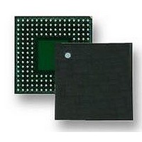
LH7A404N0F000B3 NXP Semiconductors, LH7A404N0F000B3 Datasheet - Page 54

LH7A404N0F000B3
Manufacturer Part Number
LH7A404N0F000B3
Description
MCU ARM9, LCD CTRL, SMD, LFBGA-324
Manufacturer
NXP Semiconductors
Datasheet
1.LH7A404N0F000B3.pdf
(75 pages)
Specifications of LH7A404N0F000B3
Core Size
32bit
No. Of I/o's
64
Ram Memory Size
80KB
Cpu Speed
200MHz
Oscillator Type
External Only
No. Of Timers
3
No. Of Pwm Channels
4
Digital Ic Case Style
LFBGA
Supply Voltage Range
3V
Controller Family/series
LH7A
Peripherals
ADC, DMA, RTC
Rohs Compliant
Yes
Data Bus Width
32 bit
Program Memory Type
ROMLess
Data Ram Size
80 KB
Interface Type
EBI , IrDA , JTAG , PS2 , SCI , UART , USB
Maximum Clock Frequency
200 MHz
Number Of Programmable I/os
64
Number Of Timers
3
Maximum Operating Temperature
+ 85 C
Mounting Style
SMD/SMT
Package / Case
LFBGA
Minimum Operating Temperature
- 40 C
On-chip Adc
10 bit, 9 Channel
Lead Free Status / RoHS Status
Lead free / RoHS Compliant
Available stocks
Company
Part Number
Manufacturer
Quantity
Price
Company:
Part Number:
LH7A404N0F000B3
Manufacturer:
AD
Quantity:
5 742
Company:
Part Number:
LH7A404N0F000B3,55
Manufacturer:
NXP Semiconductors
Quantity:
10 000
LH7A404
PC Card (PCMCIA) Waveforms
transactions and Figure 34 shows the waveforms and
timing for Write transactions. Figure 35 shows the pre-
charge, access, and hold timing relationships.
54
Figure 33 shows the waveforms for PCMCIA Read
NOTES:
1. Precharge time, access time, and hold
2.
time are programmable wait-state times.
nPCCE1
0
0
1
1
nPCCE2
0
1
0
1
(See Note 2)
nPCCEx
nPCREG
nPCOE/
nPCIOR
TRANSFER TYPE
D[31:0]
A[25:0]
PCDIR
Common Memory
Attribute Memory
HCLK
None
I/O
tOVDREG
tOVPCD
tOVCEx
tISD
tOVOE
Figure 33. PCMCIA Read Transfer
PRECHARGE
(See Note 1)
NXP Semiconductors
tOHOE
TIME
tIHD
tOHDREG
tOHPCD
ADDRESS
tOHCEx
DATA
(See Note 1)
ACCESS
TIME
(See Note 1)
HOLD
TIME
32-Bit System-on-Chip
Preliminary data sheet
LH7A404-15


