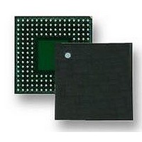
LH7A404N0F000B3 NXP Semiconductors, LH7A404N0F000B3 Datasheet - Page 31

LH7A404N0F000B3
Manufacturer Part Number
LH7A404N0F000B3
Description
MCU ARM9, LCD CTRL, SMD, LFBGA-324
Manufacturer
NXP Semiconductors
Datasheet
1.LH7A404N0F000B3.pdf
(75 pages)
Specifications of LH7A404N0F000B3
Core Size
32bit
No. Of I/o's
64
Ram Memory Size
80KB
Cpu Speed
200MHz
Oscillator Type
External Only
No. Of Timers
3
No. Of Pwm Channels
4
Digital Ic Case Style
LFBGA
Supply Voltage Range
3V
Controller Family/series
LH7A
Peripherals
ADC, DMA, RTC
Rohs Compliant
Yes
Data Bus Width
32 bit
Program Memory Type
ROMLess
Data Ram Size
80 KB
Interface Type
EBI , IrDA , JTAG , PS2 , SCI , UART , USB
Maximum Clock Frequency
200 MHz
Number Of Programmable I/os
64
Number Of Timers
3
Maximum Operating Temperature
+ 85 C
Mounting Style
SMD/SMT
Package / Case
LFBGA
Minimum Operating Temperature
- 40 C
On-chip Adc
10 bit, 9 Channel
Lead Free Status / RoHS Status
Lead free / RoHS Compliant
Available stocks
Company
Part Number
Manufacturer
Quantity
Price
Company:
Part Number:
LH7A404N0F000B3
Manufacturer:
AD
Quantity:
5 742
Company:
Part Number:
LH7A404N0F000B3,55
Manufacturer:
NXP Semiconductors
Quantity:
10 000
32-Bit System-on-Chip
Power Supply Sequencing
energized before the 3.3 V supply. If this is not possi-
ble, the 1.8 V supply may not lag the 3.3 V supply by
more than 100 µs. If longer delay time is needed, it is
recommended that the voltage difference between the
two power supplies be within 1.5 V during power supply
ramp up.
DC Specifications
NOTES:
1. Output Drive 5 can sink 20 mA of current, but sources 12 mA of current.
2. Current consumption until oscillators are stabilized.
3. See ’Current Consumption by Operating Mode’, page 34 for operating conditions.
4. Both oscillators running, LCD Active; all other peripherals stopped.
5. 32 kHz oscillator running; all other peripherals stopped.
Preliminary data sheet
VIH
VIL
VHST
VOH
VOL
IIN
IOZ
ISTARTUP
CIN
COUT
IACTIVE
IHALT
ISTANDBY
IACTIVE
IHALT
IHALT
SYMBOL
NXP recommends that the 1.8 V power supply be
CMOS/Schmitt Trigger Input HIGH Voltage
CMOS/Schmitt Trigger Input LOW Voltage
Schmitt Trigger Hysteresis
CMOS Output HIGH Voltage, Output Drive 1
Output Drive 2
Output Drive 3
Output Drive 4 and 5
CMOS Output LOW Voltage, Output Drive 1
Output Drive 2
Output Drive 3
Output Drive 4
Output Drive 5
Input Leakage Current
Input Leakage Current, with pullup resistors
Output Tri-state Leakage Current
Startup Current
Input Capacitance
Output Capacitance
Active Current (Operating Current)
Halt Current
Standby Current
Active Current (Operating Current)
Halt Current
Standby Current
PARAMETER
LH7A404-N0E-000-XX AND LH7A404-N0F-000-XX ONLY
LH7A404-N0E-092-XX AND LH7A404-N0F-092-XX ONLY
NXP Semiconductors
MIN.
0.25
-10
-95
-10
2.0
2.6
2.6
2.6
2.6
should be applied to input pins only after the device is
powered-on as described above.
DC/AC SPECIFICATIONS
below. Parameters apply to all part numbers except
where noted.
To avoid a potential latchup condition, voltage
The DC and AC specifications appears in the table
TYP.
147
228
200
41
70
60
MAX.
238
370
0.8
0.4
0.4
0.4
0.4
0.4
10
10
10
50
45
4
4
UNIT
mA
mA
mA
mA
µA
µA
µA
µA
µA
µA
pF
pF
V
V
V
V
V
V
V
V
V
V
V
V
VOUT = VDD or GND
VIN = VDD or GND
CONDITIONS
IOH = -12 mA
IOL = 12 mA
IOL = 20 mA
IOH = -2 mA
IOH = -4 mA
IOH = -8 mA
IOL = 2 mA
IOL = 4 mA
IOL = 8 mA
VIL to VIH
LH7A404
NOTE
1
1
2
3
4
5
3
4
5
31


