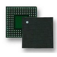
LH7A404N0F000B3 NXP Semiconductors, LH7A404N0F000B3 Datasheet - Page 29

LH7A404N0F000B3
Manufacturer Part Number
LH7A404N0F000B3
Description
MCU ARM9, LCD CTRL, SMD, LFBGA-324
Manufacturer
NXP Semiconductors
Datasheet
1.LH7A404N0F000B3.pdf
(75 pages)
Specifications of LH7A404N0F000B3
Core Size
32bit
No. Of I/o's
64
Ram Memory Size
80KB
Cpu Speed
200MHz
Oscillator Type
External Only
No. Of Timers
3
No. Of Pwm Channels
4
Digital Ic Case Style
LFBGA
Supply Voltage Range
3V
Controller Family/series
LH7A
Peripherals
ADC, DMA, RTC
Rohs Compliant
Yes
Data Bus Width
32 bit
Program Memory Type
ROMLess
Data Ram Size
80 KB
Interface Type
EBI , IrDA , JTAG , PS2 , SCI , UART , USB
Maximum Clock Frequency
200 MHz
Number Of Programmable I/os
64
Number Of Timers
3
Maximum Operating Temperature
+ 85 C
Mounting Style
SMD/SMT
Package / Case
LFBGA
Minimum Operating Temperature
- 40 C
On-chip Adc
10 bit, 9 Channel
Lead Free Status / RoHS Status
Lead free / RoHS Compliant
Available stocks
Company
Part Number
Manufacturer
Quantity
Price
Company:
Part Number:
LH7A404N0F000B3
Manufacturer:
AD
Quantity:
5 742
Company:
Part Number:
LH7A404N0F000B3,55
Manufacturer:
NXP Semiconductors
Quantity:
10 000
32-Bit System-on-Chip
ELECTRICAL SPECIFICATIONS
IMPORTANT: The LH7A404 is an electrostatic discharge (ESD) sensitive device. ESD protection circuitry internal to the LH7A404 has been
Absolute maximum ratings
NOTE: These stress ratings are only for transient conditions. Operation at or beyond absolute
Recommended operating conditions for LH7A404-N0E-000-xx/LH7A404-N0F-000-xx
NOTES:
1. Core Voltage should never exceed I/O Voltage after initial power up. See “Power Supply Sequencing” on page 31.
2. Many of the peripherals do not operate properly at clock speeds other than 14.7456 MHz. Some
Preliminary data sheet
DC Core Supply Voltage (VDDC)
DC I/O Supply Voltage (VDD)
DC Analog Supply Voltage (VDDA)
DC Analog Supply Voltage (VDDAD)
5 V Tolerant Digital Input Pin Voltage
ESD, Human Body Model (Analog pins AN0 - AN9 rated at 500 V)
ESD, Charged Device Model
Storage Temperature
DC Core Supply Voltage (VDDC)
DC I/O Supply Voltage (VDD)
DC Analog Supply Voltage (VDDA)
DC A/D and TSC Supply Voltage (VDDAD)
Clock Frequency
Bus Clock Frequency
External Clock Input (XTALIN)
External Clock Input (XTALIN) Voltage
Operating Temperature
(such as USB) function only at 14.7456 MHz.
maximum rating conditions may affect reliability and cause permanent damage to the device.
added to reduce ESD susceptibility. Appropriate ESD precautions are still required during handling to prevent degradation or
failure due to high electrostatic discharges. System design practices should be evaluated to prevent LH7A404 ESD voltages
from exceeding the maximum rated voltage as specified in this data sheet.
PARAMETER
PARAMETER
MINIMUM
14 MHz
10 MHz
1.71 V
1.71 V
1.71 V
−40°C
3.0 V
3.0 V
NXP Semiconductors
14.7456 MHz
TYPICAL
1.8 V
3.3 V
1.8 V
3.3 V
1.8 V
25°C
MINIMUM MAXIMUM
−0.3 V
−0.3 V
−0.3 V
−0.3 V
−0.5 V
−55°C
MAXIMUM NOTES
200 MHz
100 MHz
20 MHz
1.89 V
1.89 V
1.89 V
+85°C
3.6 V
3.6 V
125°C
2.4 V
4.6 V
2.4 V
4.6 V
5.5 V
2 kV
1 kV
1
2
LH7A404
29


