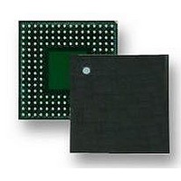
LH7A404N0F000B3 NXP Semiconductors, LH7A404N0F000B3 Datasheet - Page 63

LH7A404N0F000B3
Manufacturer Part Number
LH7A404N0F000B3
Description
MCU ARM9, LCD CTRL, SMD, LFBGA-324
Manufacturer
NXP Semiconductors
Datasheet
1.LH7A404N0F000B3.pdf
(75 pages)
Specifications of LH7A404N0F000B3
Core Size
32bit
No. Of I/o's
64
Ram Memory Size
80KB
Cpu Speed
200MHz
Oscillator Type
External Only
No. Of Timers
3
No. Of Pwm Channels
4
Digital Ic Case Style
LFBGA
Supply Voltage Range
3V
Controller Family/series
LH7A
Peripherals
ADC, DMA, RTC
Rohs Compliant
Yes
Data Bus Width
32 bit
Program Memory Type
ROMLess
Data Ram Size
80 KB
Interface Type
EBI , IrDA , JTAG , PS2 , SCI , UART , USB
Maximum Clock Frequency
200 MHz
Number Of Programmable I/os
64
Number Of Timers
3
Maximum Operating Temperature
+ 85 C
Mounting Style
SMD/SMT
Package / Case
LFBGA
Minimum Operating Temperature
- 40 C
On-chip Adc
10 bit, 9 Channel
Lead Free Status / RoHS Status
Lead free / RoHS Compliant
Available stocks
Company
Part Number
Manufacturer
Quantity
Price
Company:
Part Number:
LH7A404N0F000B3
Manufacturer:
AD
Quantity:
5 742
Company:
Part Number:
LH7A404N0F000B3,55
Manufacturer:
NXP Semiconductors
Quantity:
10 000
32-Bit System-on-Chip
Clock and State Controller
(CSC) Waveforms
coming out of Reset or Power-On. Table 13 gives the
timing parameters.
32.768 kHz oscillator is stable, and must be deasserted
at least two 1 Hz clock periods before the WAKEUP
signal is asserted. Once the 14.7456 MHz oscillator is
stable, the PLLs require 250 µs to lock.
Boot), the Wakeup pin must not be asserted for two 1
NOTE: *VDDC = VDDCmin
NOTE: *The timing relationship is specified as a cycle-based timing. Due to variations in crystal input clock jitter,
Preliminary data sheet
tOSC32 (32 kHz)
tOSC14 (14 MHz)
Figure 48 shows the behavior of the LH7A404 when
At Power-On, nPOR must be held LOW until the
On transition from Standby to Run (including a Cold
PARAMETER
power rail noise and I/O conditioning these timings will vary marginally. It is recommended that designers
WAKEUP
XTAL32
XTAL14
VDDC
nPOR
VDDCmin
32.768 kHz Oscillator Stabilization Time after Power On*
14.7456 MHz Oscillator Stabilization Time after WAKEUP
tOSC32
DESCRIPTION
Table 13. Reset AC Timing
Figure 48. PLL Start-up
NXP Semiconductors
tOSC14
Hz clock periods after assertion of nPOR to allow time
for sampling BATOK and nEXTPWR. The delay
prevents a false ‘battery good’ indication caused by
alkaline battery recovery that can immediately follow a
battery-low switch off.
nRESETOUT Timing Sequence
each of the three reset triggers (nPOR, nURESET, and
nPWRFL) in Figure 49 through Figure 51, and timing
values are presented in Table 14 through Table 16.
Timing for the nRESETOUT sequence is shown for
MIN. MAX.
550
2.5
UNIT
ms
ms
LH7A404
LH7A404-22
63


