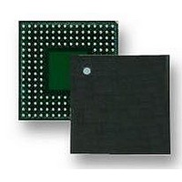
LH7A404N0F000B3 NXP Semiconductors, LH7A404N0F000B3 Datasheet - Page 20

LH7A404N0F000B3
Manufacturer Part Number
LH7A404N0F000B3
Description
MCU ARM9, LCD CTRL, SMD, LFBGA-324
Manufacturer
NXP Semiconductors
Datasheet
1.LH7A404N0F000B3.pdf
(75 pages)
Specifications of LH7A404N0F000B3
Core Size
32bit
No. Of I/o's
64
Ram Memory Size
80KB
Cpu Speed
200MHz
Oscillator Type
External Only
No. Of Timers
3
No. Of Pwm Channels
4
Digital Ic Case Style
LFBGA
Supply Voltage Range
3V
Controller Family/series
LH7A
Peripherals
ADC, DMA, RTC
Rohs Compliant
Yes
Data Bus Width
32 bit
Program Memory Type
ROMLess
Data Ram Size
80 KB
Interface Type
EBI , IrDA , JTAG , PS2 , SCI , UART , USB
Maximum Clock Frequency
200 MHz
Number Of Programmable I/os
64
Number Of Timers
3
Maximum Operating Temperature
+ 85 C
Mounting Style
SMD/SMT
Package / Case
LFBGA
Minimum Operating Temperature
- 40 C
On-chip Adc
10 bit, 9 Channel
Lead Free Status / RoHS Status
Lead free / RoHS Compliant
Available stocks
Company
Part Number
Manufacturer
Quantity
Price
Company:
Part Number:
LH7A404N0F000B3
Manufacturer:
AD
Quantity:
5 742
Company:
Part Number:
LH7A404N0F000B3,55
Manufacturer:
NXP Semiconductors
Quantity:
10 000
LH7A404
AMBA APB BUS
peripherals accessed less frequently. This reduces the
loading on the AHB, allowing it to run faster to maxi-
mize system performance, while the APB can operate
at a lower clock rate to conserve power. The APB
Bridge is the only master on the APB. All AHB masters
can access APB peripherals via the ABP Bridge. The
APB clock frequency can be selected by software to
divide the clock speed of the AHB bus by 2, 4, or 8.
EXTERNAL BUS INTERFACE (EBI)
wide, high speed gateway to external memory devices.
The supported memory devices include:
• Asynchronous RAM/ROM/Flash
• Synchronous DRAM/Flash
• PCMCIA interfaces
• CompactFlash interfaces.
nous Memory Controller or Synchronous Memory Con-
troller. There is an arbiter on the EBI input, with priority
given to the Synchronous Memory Controller interface.
LCD BUS
that connects it to the system’s embedded memory and
external SDRAM. The function of this local data bus is
to allow the LCD controller to perform its video refresh
function without congesting the main AHB bus. This
leads to better system performance and lower power
consumption. There is an arbiter on both the embed-
ded memory and the synchronous memory controller.
In both cases the LCD bus is given priority.
DMA BUSES
higher speed/higher data volume APB peripherals
(MMC, USB Device and AC97) to the AHB bus. This
enables the efficient transfer of data between these
peripherals and external memory without the interven-
tion of the ARM922T core.
20
The AMBA APB provides a lower-bandwidth bus for
The External Bus Interface (EBI) provides a 32-bit-
The EBI can be controlled by either the Asynchro-
The LCD controller has its own local memory bus
The LH7A404 has a DMA system that connects the
NXP Semiconductors
USB HOST CONTROLLER DMA BUS
ler. It acts as another bus master on the AHB bus. It
does not interact with the non-USB DMA controller
except in bus arbitration.
Memory Map
allowing addressing up to 4GB of memory. This mem-
ory space is subdivided into a number of memory
banks, shown in Figure 4. Four of these banks (each
256MB) are allocated to the Synchronous Memory
Controller. Eight banks (each 256MB) are allocated to
the Asynchronous Memory Controller. Two of these
eight banks are designed for PCMCIA systems. Part of
the remaining memory space is allocated to the embed-
ded SRAM, and to the control registers of the AHB and
APB. The rest of the memory space is not used.
nal devices. The selection is determined by the value of
five pins at power-on reset as shown in Table 6. If boot-
ing is from an external device (with INTBOOT = 0),
refer to Table 7. When booting from external synchro-
nous memory, bank 4 (nSCS3) is mapped into memory
location zero. When booting from external asynchro-
nous memory, memory bank 0 (nSCS0) is mapped into
memory location zero.
system for the two boot modes.
configure the ARM922T MMU to remap the low mem-
ory space to a location in RAM. This allows the user to
set the interrupt vector table.
The USB Host Controller has its own DMA control-
The LH7A404 system has a 32-bit-wide address bus,
The LH7A404 can boot from both internal and exter-
Figure 4 shows the memory map of the LH7A404
Once the LH7A404 has booted, the boot code can
32-Bit System-on-Chip
Preliminary data sheet


