AD9957/PCBZ Analog Devices Inc, AD9957/PCBZ Datasheet - Page 10
AD9957/PCBZ
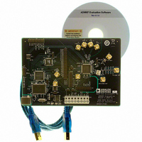
Manufacturer Part Number
AD9957/PCBZ
Description
D/A Converter Evaluation Board
Manufacturer
Analog Devices Inc
Series
AgileRF™r
Datasheet
1.AD9957BSVZ-REEL.pdf
(64 pages)
Specifications of AD9957/PCBZ
Silicon Manufacturer
Analog Devices
Application Sub Type
Direct Digital Synthesizer
Kit Application Type
Clock & Timing
Silicon Core Number
AD9957
Kit Contents
Board
Main Purpose
Timing: DDS Modulators
Embedded
No
Utilized Ic / Part
AD9957
Primary Attributes
14-Bit DAC, 32-Bit Tuning Word Width
Secondary Attributes
1GHz, Graphical User Interface
Lead Free Status / RoHS Status
Lead free / RoHS Compliant
Available stocks
Company
Part Number
Manufacturer
Quantity
Price
Company:

Part Number:
AD9957/PCBZ
Manufacturer:
LT
Quantity:
962


AD9957
Table 3. Pin Function Descriptions
Pin No.
1, 24, 61, 72, 86,
87, 93, 97 to 100
2
3, 6, 89, 92
74 to 77, 83
17, 23, 30, 47, 57,
64
11, 15, 21, 28, 45,
56, 66
4, 5, 73, 78, 79,
82, 85, 88, 96
13, 16, 22, 29, 46,
58, 62, 63, 65
7
8
9
10
12
14
18
19
20
25 to 27, 31 to
39, 42 to 44, 48
to 50
42
43
40
41
41
51
52 to 54
55
Mnemonic
NC
PLL_LOOP_FILTER
AVDD (1.8V)
AVDD (3.3V)
DVDD (1.8V)
DVDD_I/O (3.3V)
AGND
DGND
SYNC_IN+
SYNC_IN−
SYNC_OUT+
SYNC_OUT−
SYNC_SMP_ERR
MASTER_RESET
EXT_PWR_DWN
PLL_LOCK
CCI_OVFL
D<17:0>
SPORT I-DATA
SPORT Q-DATA
PDCLK
TxENABLE
FS
RT
PROFILE<2:0>
SYNC_CLK
I/O
I
I
I
I
I
I
I
I
I
O
O
O
I
I
O
O
I/O
I
I
O
I
I
I
I
O
1
Description
Not Connected. Allow device pin to float.
PLL-Loop Filter Compensation. See External PLL Loop Filter Components section.
Analog Core VDD. 1.8 V analog supplies.
Analog DAC VDD. 3.3 V analog supplies.
Digital Core VDD. 1.8 V digital supplies.
Digital Input/Output VDD. 3.3 V digital supplies.
Analog Ground.
Digital Ground.
Synchronization Signal, Digital Input (Rising Edge Active). Synchronization signal from
external master to synchronize internal subclocks. See the Synchronization of Multiple
Devices section.
Synchronization Signal, Digital Input (Falling Edge Active). Synchronization signal from
external master to synchronize internal subclocks. See the Synchronization of Multiple
Devices section.
Synchronization Signal, Digital Output (Rising Edge Active). Synchronization signal from
internal device subclocks to synchronize external slave devices. See the Synchronization of
Multiple Devices section.
Synchronization Signal, Digital Output (Falling Edge Active). Synchronization signal from
internal device subclocks to synchronize external slave devices. See the Synchronization of
Multiple Devices section.
Synchronization Sample Error, Digital Output (Active High). A high on this pin indicates
that the AD9957 did not receive a valid sync signal on SYNC_IN+/SYNC_IN−. See the
Synchronization of Multiple Devices section.
Master Reset, Digital Input (Active High). This pin clears all memory elements and sets
registers to default values.
External Power-Down, Digital Input (Active High). A high level on this pin initiates the
currently programmed power-down mode. See the Power-Down Control section for
further details. If unused, tie to ground.
PLL Lock, Digital Output (Active High). A high on this pin indicates that the clock multiplier
PLL has acquired lock to the reference clock input.
CCI Overflow Digital Output, Active High. A high on this pin indicates a CCI filter overflow.
This pin remains high until the CCI overflow condition is cleared.
Parallel Data Input Bus (Active High). These pins provide the interleaved, 18-bit, digital, I
and Q vectors for the modulator to upconvert. Also used for a GPIO port in Blackfin
interface mode.
In Blackfin interface mode, this pin serves as the I-data serial input.
In Blackfin interface mode, this pin serves as the Q-data serial input.
Parallel Data Clock, Digital Output (Clock). See the Signal Processing section for details.
Transmit Enable, Digital Input (Active High). See the Signal Processing section for details.
FS Input. In Blackfin interface mode, this pin serves as the FS input to receive the RFS
output signal from the Blackfin.
RAM Trigger, Digital Input (Active High). This pin provides control for the RAM amplitude
scaling function. When this function is engaged, a high sweeps the amplitude from the
beginning RAM address to the end. A low sweeps the amplitude from the end RAM
address to the beginning. If unused, connect to ground or supply.
Profile Select Pins, Digital Inputs (Active High). These pins select one of eight
phase/frequency profiles for the DDS core (single tone or carrier tone). Changing the state
of one of these pins transfers the current contents of all I/O buffers to the corresponding
registers. State changes should be set up to the SYNC_CLK pin.
Output System Clock/4, Digital Output (Clock). The I/O_UPDATE and PROFILE<2:0> pins
should be set up to the rising edge of this signal.
Rev. B | Page 10 of 64
Related parts for AD9957/PCBZ
Image
Part Number
Description
Manufacturer
Datasheet
Request
R


Part Number:
Description:
±1.7g Dual-Axis IMEMS Accelerometer Evaluation Board
Manufacturer:
Analog Devices Inc
Datasheet:

Part Number:
Description:
Inertial Sensor Evaluation System
Manufacturer:
Analog Devices Inc
Datasheet:
Part Number:
Description:
Manufacturer:
Analog Devices Inc
Datasheet:
Part Number:
Description:
Manufacturer:
Analog Devices Inc
Datasheet:
Part Number:
Description:
Manufacturer:
Analog Devices Inc
Datasheet:
Part Number:
Description:
Manufacturer:
Analog Devices Inc
Datasheet:
Part Number:
Description:
Manufacturer:
Analog Devices Inc
Datasheet:
Part Number:
Description:
Manufacturer:
Analog Devices Inc
Datasheet:
Part Number:
Description:
Manufacturer:
Analog Devices Inc
Datasheet:
Part Number:
Description:
Manufacturer:
Analog Devices Inc
Datasheet:
Part Number:
Description:
Manufacturer:
Analog Devices Inc
Datasheet:
Part Number:
Description:
Manufacturer:
Analog Devices Inc
Datasheet: