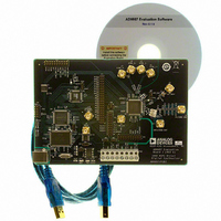
AD9957/PCBZ Analog Devices Inc, AD9957/PCBZ Datasheet - Page 23

AD9957/PCBZ
Manufacturer Part Number
AD9957/PCBZ
Description
D/A Converter Evaluation Board
Manufacturer
Analog Devices Inc
Series
AgileRF™r
Datasheet
1.AD9957BSVZ-REEL.pdf
(64 pages)
Specifications of AD9957/PCBZ
Silicon Manufacturer
Analog Devices
Application Sub Type
Direct Digital Synthesizer
Kit Application Type
Clock & Timing
Silicon Core Number
AD9957
Kit Contents
Board
Main Purpose
Timing: DDS Modulators
Embedded
No
Utilized Ic / Part
AD9957
Primary Attributes
14-Bit DAC, 32-Bit Tuning Word Width
Secondary Attributes
1GHz, Graphical User Interface
Lead Free Status / RoHS Status
Lead free / RoHS Compliant
Available stocks
Company
Part Number
Manufacturer
Quantity
Price
Company:
Part Number:
AD9957/PCBZ
Manufacturer:
LT
Quantity:
962
Encoding and pulse shaping of symbols must be implemented
before the data is presented to the input of the AD9957. Data
delivered to the input of the AD9957 may be formatted as either
twos complement or offset binary (see the Data Format bit in
Table 13). In BFI mode, the bit sequence order can be set to
either MSB-first or LSB-first (via the Blackfin Bit Order bit).
INVERSE CCI FILTER
The inverse cascaded comb integrator (CCI) filter predistorts
the data, compensating for the slight attenuation gradient imposed
by the CCI filter (see the Programmable Interpolating Filter
section). Data entering the first half-band filter occupies a maxi-
mum bandwidth of ½ f
sample rate at the input of the first half-band filter); see Figure 33.
If the CCI filter is used, the inband attenuation gradient can pose a
problem for applications requiring an extremely flat pass band.
For example, if the spectrum of the data supplied to the AD9957
occupies a significant portion of the ½ f
frequencies of the data spectrum are slightly more attenuated
than the lower frequencies (the worst-case overall droop from
f = 0 to ½ f
characteristic that is the inverse of the CCI filter response over
the ½ f
The product of the two responses yields an extremely flat
pass band (±0.05 dB over the baseband Nyquist bandwidth)
eliminating the inband attenuation gradient introduced by the
CCI filter. The cost is a slight attenuation of the input signal
(approximately 0.5 dB for a CCI interpolation rate of 2, and
0.8 dB for higher interpolation rates).
The inverse CCI filter can be bypassed using the appropriate bit
in the register map; it is automatically bypassed if the CCI inter-
polation rate is 1×. When bypassed, power to the stage turns off
to reduce power consumption.
IQ
INBAND
ATTENUATION
GRADIENT
region.
DATA
½f
IQ
is <0.8 dB). The inverse CCI filter has a response
f
IQ
Figure 33. CCI Filter Response
IQ
as defined by Nyquist (where f
CCI FILTER RESPONSE
DATA
region, the higher
4
f
IQ
f
IQ
is the
Rev. B | Page 23 of 64
FIXED INTERPOLATOR (4×)
This block is a fixed 4× rate interpolator, implemented as a
cascade of two half-band filters. Together, the sampling rate
of these two filters increases by a factor of four while preserving
the spectrum of the baseband signal applied at the input. Both
are linear phase filters; virtually no phase distortion is intro-
duced within their pass bands. Their combined insertion loss
is 0.01 dB, preserving the relative amplitude of the input signal.
The filters are designed to deliver a composite performance that
yields a usable pass band of 40% of the input sample rate. Within
that pass band, ripple does not exceed 0.002 dB peak-to-peak.
The stop band extends from 60% to 340% of the input sample
rate and offers a minimum of 85 dB attenuation. Figure 34 and
Figure 35 show the composite response of the two half-band filters.
In BFI mode, there are two additional half-band filters resident,
yielding a total fixed interpolation factor of 16×. The extra BFI
filters use the same filter tap coefficient values as the QDUC
half-band filters, but their data pathway is 16 bits (instead of
18 bits as with the QDUC half-band filters). As such, baseband
quantization noise is higher in BFI mode.
–0.002
–0.004
–0.006
–0.008
–0.010
0.010
0.008
0.006
0.004
0.002
Figure 34. Half-Band 1 and Half-Band 2 Composite Response
–100
–110
–120
–10
–20
–30
–40
–50
–60
–70
–80
–90
10
(Frequency Scaled to Input Sample Rate of Half-Band 1)
(Frequency Scaled to Input Sample Rate of Half-Band 1)
0
0
0
0
Figure 35. Composite Pass-Band Detail
0.5
0.1
1.0
1.5
0.2
2.0
f
f
I
I
0.3
2.5
3.0
0.4
3.5
AD9957
0.5
4.0


