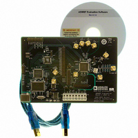
AD9957/PCBZ Analog Devices Inc, AD9957/PCBZ Datasheet - Page 28
AD9957/PCBZ
Manufacturer Part Number
AD9957/PCBZ
Description
D/A Converter Evaluation Board
Manufacturer
Analog Devices Inc
Series
AgileRF™r
Datasheet
1.AD9957BSVZ-REEL.pdf
(64 pages)
Specifications of AD9957/PCBZ
Silicon Manufacturer
Analog Devices
Application Sub Type
Direct Digital Synthesizer
Kit Application Type
Clock & Timing
Silicon Core Number
AD9957
Kit Contents
Board
Main Purpose
Timing: DDS Modulators
Embedded
No
Utilized Ic / Part
AD9957
Primary Attributes
14-Bit DAC, 32-Bit Tuning Word Width
Secondary Attributes
1GHz, Graphical User Interface
Lead Free Status / RoHS Status
Lead free / RoHS Compliant
Available stocks
Company
Part Number
Manufacturer
Quantity
Price
Company:

Part Number:
AD9957/PCBZ
Manufacturer:
LT
Quantity:
962


AD9957
LOAD/RETRIEVE RAM OPERATION
Loading or retrieving the RAM contents is a three-step process.
1.
2.
3.
Figure 40 shows the RAM block diagram when used for loading
or retrieve operations.
During a load or retrieve operation, the state machine controls
an up/down counter to step through the required RAM locations.
The counter is synchronized with the serial I/O port so that the
serial/parallel conversion of the 32-bit words is correctly timed
with the generation of the appropriate RAM address to properly
execute the desired read or write operation. The up/down
counter always increments through the address range during
serial I/O port operations.
Because the RAM segment registers are completely independent,
it is possible to define overlapping address ranges. However,
doing so causes the overlapping address locations to be over-
written by the most recent write operation. It is recommended
that the user avoid defining overlapping address ranges.
RAM PLAYBACK OPERATION
When the RAM has been loaded, it can be used for playback
operation. The destination of the playback data is selected via
the RAM playback destination bit. The active RAM segment
register is selected by the appropriate transition of the RT pin.
The active RAM segment register directs the internal state
machine by defining the RAM address range occupied by the
data and the RAM playback mode. It also defines the playback
NOTES
1. NONESSENTIAL FUNCTIONAL COMPONENTS ARE RENDERED IN GRAY.
MACHINE
STATE
Program the RAM segment registers with start and end
addresses defining the boundaries of each independent
RAM segment.
Toggle the RT pin with the appropriate transition to select
the desired RAM segment register.
Using the serial I/O port, write (or read) the address range
specified by the selected RAM segment register.
CLK
16
10
UP/DOWN COUNTER
10
3
RAM MODE
ADDRESS STEP RATE
START ADDRESS
END ADDRESS
Figure 40. RAM Load/Retrieve Operation
U/D
Q CHANNEL
Q
I CHANNEL
10
DDS CLOCK
BASEBAND DATA CLOCK
RAM
QS
IS
Q
I
(MSBs)
(LSBs)
32
16
16
32
REGISTERS
SEGMENT
RAM
RT
SDIO
SDO
SCLK
I/O_RESET
CS
Rev. B | Page 28 of 64
rate when the playback destination is the baseband scaling
multipliers.
Although RAM load/retrieve operations via the serial I/O port
take precedence over playback, it is recommended that the user
not attempt RAM access via the serial I/O port when the RAM
enable bit is set.
Figure 41 is a block diagram showing the functional compo-
nents used for RAM playback operation when the internal
destination is the baseband scaling multipliers.
During playback to the baseband scaling multipliers, the
address step rate word in the active RAM segment register sets
the rate at which RAM data samples are delivered to the
multipliers. The following equations define the RAM sample
rate and sample interval (Δt):
where:
R is the rate interpolation factor for the CCI filter.
M is the 16-bit value of the address step rate word stored in the
active RAM segment register.
If the RAM enable bit is set and the baseband scaling multi-
pliers are selected as the playback destination, then assertion
of an I/O update or profile change causes the multipliers to be
driven with a static value of zero. A subsequent state change on
the RT pin causes the multipliers to be driven by the data played
back from the RAM instead of the static zero value.
Figure 42 is a block diagram showing RAM playback operation
when the internal destination is the baseband data path. During
playback to the baseband data path, the state machine increments/
decrements the RAM address at the baseband data rate (the
address step rate must be set to 1).
NOTES
1. NONESSENTIAL FUNCTIONAL COMPONENTS ARE RENDERED IN GRAY.
MACHINE
STATE
RAM
∆
t
=
CLK
Figure 41. RAM Playback to Baseband Scaling Multipliers
10
16
UP/DOWN COUNTER
f
Sample
4
10
SYSCLK
3
RM
RAM MODE
ADDRESS STEP RATE
START ADDRESS
END ADDRESS
U/D
Q CHANNEL
Q
I CHANNEL
Rate
10
=
DDS CLOCK
BASEBAND DATA CLOCK
RAM
f
QS
4
SYSCLK
IS
Q
RM
I
(MSBs)
(LSBs)
32
16
16
32
REGISTERS
SEGMENT
RAM
RT
SDIO
SDO
SCLK
I/O_RESET
CS
Related parts for AD9957/PCBZ
Image
Part Number
Description
Manufacturer
Datasheet
Request
R


Part Number:
Description:
±1.7g Dual-Axis IMEMS Accelerometer Evaluation Board
Manufacturer:
Analog Devices Inc
Datasheet:

Part Number:
Description:
Inertial Sensor Evaluation System
Manufacturer:
Analog Devices Inc
Datasheet:
Part Number:
Description:
Manufacturer:
Analog Devices Inc
Datasheet:
Part Number:
Description:
Manufacturer:
Analog Devices Inc
Datasheet:
Part Number:
Description:
Manufacturer:
Analog Devices Inc
Datasheet:
Part Number:
Description:
Manufacturer:
Analog Devices Inc
Datasheet:
Part Number:
Description:
Manufacturer:
Analog Devices Inc
Datasheet:
Part Number:
Description:
Manufacturer:
Analog Devices Inc
Datasheet:
Part Number:
Description:
Manufacturer:
Analog Devices Inc
Datasheet:
Part Number:
Description:
Manufacturer:
Analog Devices Inc
Datasheet:
Part Number:
Description:
Manufacturer:
Analog Devices Inc
Datasheet:
Part Number:
Description:
Manufacturer:
Analog Devices Inc
Datasheet: