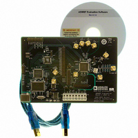
AD9957/PCBZ Analog Devices Inc, AD9957/PCBZ Datasheet - Page 42

AD9957/PCBZ
Manufacturer Part Number
AD9957/PCBZ
Description
D/A Converter Evaluation Board
Manufacturer
Analog Devices Inc
Series
AgileRF™r
Datasheet
1.AD9957BSVZ-REEL.pdf
(64 pages)
Specifications of AD9957/PCBZ
Silicon Manufacturer
Analog Devices
Application Sub Type
Direct Digital Synthesizer
Kit Application Type
Clock & Timing
Silicon Core Number
AD9957
Kit Contents
Board
Main Purpose
Timing: DDS Modulators
Embedded
No
Utilized Ic / Part
AD9957
Primary Attributes
14-Bit DAC, 32-Bit Tuning Word Width
Secondary Attributes
1GHz, Graphical User Interface
Lead Free Status / RoHS Status
Lead free / RoHS Compliant
Available stocks
Company
Part Number
Manufacturer
Quantity
Price
Company:
Part Number:
AD9957/PCBZ
Manufacturer:
LT
Quantity:
962
AD9957
When a device other than another AD9957 provides the
SYNC_IN signal it must be LVDS compatible. Furthermore,
although SYNC_IN is typically considered to be a periodic
clock signal, it is not an absolute requirement. It is feasible to
drive the SYNC_IN pins with a single synchronization pulse as
long as its edge transition meets the setup/hold timing required
for the internally generated sync pulse (as detailed later in this
section). However, using a periodic SYNC_IN signal has the
distinct advantage that should any of the devices arbitrarily lose
synchronization it automatically resynchronizes with the arrival
of the next SYNC_IN edge.
The 5-bit sync receiver delay word in the multichip sync register
delays the SYNC_IN signal in steps of ~150 ps. This provides
the ability to time align the arrival of the SYNC_IN signal to
multiple devices by compensating for unequal propagation times.
The edge detection logic in the sync receiver generates a
synchronization pulse (sync pulse) having a duration of one
SYSCLK cycle with a repetition rate equal to that of the signal
applied to the SYNC_IN pins. To produce the sync pulse, the
strobe generator samples the delayed rising edge of the SYNC_IN
signal with the rising edge of the local SYSCLK. The generation
of this sync pulse is crucial to the operation of the synchroniza-
tion mechanism, because it performs the task of placing the
clock generator into a known state. The sync pulse presets the
R-divider stage of the internal clock generator, which behaves as
a presettable downcounter (see Figure 55). The programmable
6-bit sync state preset value word in the multichip sync register
establishes the preset state. The preset state is only active for a
single SYSCLK period, after which the clock generator is free to
cycle through its state sequence until the next sync pulse arrives
(see Figure 55). In addition to presetting the R-divider, the sync
pulse also synchronously presets the other dividers to a proper
state in order to preserve the cadence of the clock tree.
The ability to program the clock state preset value provides the
flexibility to synchronize devices, but with specific relative clock
state offsets by assigning a different sync state preset value word
SYNC_SMP_ERR
SYNC_IN+
SYNC_IN–
12
7
8
VALIDATION
RECEIVER
LVDS
DELAYED SYNC-IN SIGNAL
DISABLE
TIMING
SYNC
SETUP AND HOLD
VALIDATION
PROGAMMABLE
DELAY
RECEIVER
DELAY
SYNC
Figure 57. Sync Receiver
SYNC
VALIDATION
DELAY
Rev. B | Page 42 of 64
5
4
RISING EDGE
GENERATOR
RECEIVER
DETECTOR
ENABLE
STROBE
SYNC
to each device in a group. This flexibility is limited, however,
because the sync state preset value must adhere to certain
bounds to satisfy internal timing requirements. Regardless of
the programmed sync state preset value, the preset value is
internally constrained to the range, 2 to R, where R is the CCI
filter interpolation factor. A programmed value of 0 or 1 is forced
to 2, whereas a programmed value greater than R is forced to R.
SETUP/HOLD VALIDATION
Synchronization of the AD9957 internal clock generator with
other external devices relies on the ability of the sync receiver’s
edge detection circuit to generate a valid sync pulse. This
requires proper sampling of the rising edge of the delayed
SYNC_IN signal with the rising edge of the local SYSCLK. If the
edge timing of these signals fails to meet the setup or hold time
requirements of the internal latches in the edge detection
circuitry, the proper generation of a sync pulse is in jeopardy.
The setup-and-hold validation block (see Figure 58) gives the
user a means to validate that proper edge timing exists between
the two signals. The Sync Timing Validation Disable bit in
Control Function Register 2 controls whether or not the setup-
and-hold validation block is active.
The validation block makes use of a specified time window
(programmable in increments of ~150 ps via the 4-bit sync
validation delay word in the multichip sync register). The setup
validation and hold validation circuits use latches identical to
those in both the rising edge detector and strobe generator. The
programmable time window skews the timing between the local
SYSCLK signal and the delayed sync-in signal. If the hold valida-
tion and setup validation circuits fail to produce the same logic
states, it is an indication of a possible setup or hold violation.
The check logic of Figure 58 monitors the state of the setup and
hold validation latches. If they are not equal (that is, a potential
setup/hold violation exists), a Logic 1 is stored in an internal
validation result latch; otherwise, a Logic 0 is stored. The state
of validation result latch appears at the SYNC_SMP_ERR pin.
AND
PRESET VALUE
SYNC PULSE
SYNC STATE
6
GENERATOR
P
R
E
S
E
T
LOAD
CLOCK
Q
Q
.
.
.
N
0
.
.
.
CLOCK
STATE
SYSCLK
INTERNAL
CLOCKS


