AD9957/PCBZ Analog Devices Inc, AD9957/PCBZ Datasheet - Page 41
AD9957/PCBZ
Manufacturer Part Number
AD9957/PCBZ
Description
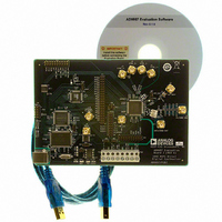
D/A Converter Evaluation Board
Manufacturer
Analog Devices Inc
Series
AgileRF™r
Datasheet
1.AD9957BSVZ-REEL.pdf
(64 pages)
Specifications of AD9957/PCBZ
Silicon Manufacturer
Analog Devices
Application Sub Type
Direct Digital Synthesizer
Kit Application Type
Clock & Timing
Silicon Core Number
AD9957
Kit Contents
Board
Main Purpose
Timing: DDS Modulators
Embedded
No
Utilized Ic / Part
AD9957
Primary Attributes
14-Bit DAC, 32-Bit Tuning Word Width
Secondary Attributes
1GHz, Graphical User Interface
Lead Free Status / RoHS Status
Lead free / RoHS Compliant
Available stocks
Company
Part Number
Manufacturer
Quantity
Price
Company:

Part Number:
AD9957/PCBZ
Manufacturer:
LT
Quantity:
962


SYSCLK
The sync generator produces an LVDS-compatible clock signal
with a 50% duty cycle that appears at the SYNC_OUT pins. The
frequency of the SYNC_OUT signal can be one of two possible
rates. With the AD9957 programmed for any of the following
modes:
•
•
•
The frequency of SYNC_OUT is given by:
With the AD9957 programmed for the QDUC or interpolating
DAC mode and with the CCI filter not bypassed (that is, R>1)
the frequency of SYNC_OUT is given by
where R is the programmed interpolation factor of the CCI filter.
The signal at the SYNC_OUT pins is edge aligned with either
the rising or falling edge of the internal SYSCLK signal as deter-
mined by the Sync Polarity bit. Because the SYNC_OUT signal is
synchronized with the internal SYSCLK of the master device, the
master device SYSCLK serves as the reference timing source for
all slave devices.
The user can adjust the output delay of the SYNC_OUT signal
in steps of ~150 ps by programming the 5-bit sync generator
delay word via the serial I/O port. The programmable output
delay facilitates added edge timing flexibility to the overall
synchronization mechanism.
Single tone mode
Quadrature modulation mode with the CCI filter bypassed
(that is, interpolation factor is 1)
Interpolating DAC mode with the CCI filter bypassed (that
is, interpolation factor is 1)
f
f
SYNC
SYNC
POLARITY
÷16
SYNC
_
_
OUT
OUT
=
=
÷2R
0
1
f
f
SYSCLK
SYSCLK
32
16
Figure 56. Sync Generator
R
GENERATOR
ENABLE
D Q
SYNC
R
PROGAMMABLE
GENERATOR
DELAY
SYNC
DELAY
5
DRIVER
LVDS
10
9
SYNC_OUT
Rev. B | Page 41 of 64
SYNC RECEIVER
The sync receiver block (shown in Figure 57) is activated via the
Sync Receiver Enable bit. The sync receiver consists of three
subsections: the input delay and edge detection block, the
internal clock generator block, and the setup-and-hold valida-
tion block.
The clock generator block remains operational even when the
sync receiver is not enabled.
The sync receiver accepts an LVDS-compatible signal at the
SYNC_IN pins. Typically, the signal applied to the SYNC_IN
pins originates from the SYNC_OUT of another AD9957
functioning as a master timing unit. The sync receiver expects a
periodic synchronization pulse that meets certain frequency
requirements based on the operating mode of the AD9957.
When programmed for single tone mode, the frequency of
SYNC_IN must satisfy
where M is any integer greater than zero. When programmed
for quadrature modulation mode (using the parallel data port)
or interpolating DAC mode, the frequency of SYNC_IN must
satisfy
where R is the programmed CCI interpolation factor and M is
any integer greater than or equal to zero. When programmed
for quadrature modulation mode using the BlackFin interface,
the frequency of SYNC_IN must satisfy
where R is the programmed CCI interpolation factor and M is
any integer greater than or equal to zero.
f
f
f
SYNC
SYNC
SYNC
_
_
_
IN
IN
IN
=
=
=
16
32
f
SYSCLK
4
f
f
(
(
SYSCLK
SYSCLK
R
M
R
+
+
M
M
)
)
AD9957
Related parts for AD9957/PCBZ
Image
Part Number
Description
Manufacturer
Datasheet
Request
R


Part Number:
Description:
±1.7g Dual-Axis IMEMS Accelerometer Evaluation Board
Manufacturer:
Analog Devices Inc
Datasheet:

Part Number:
Description:
Inertial Sensor Evaluation System
Manufacturer:
Analog Devices Inc
Datasheet:
Part Number:
Description:
Manufacturer:
Analog Devices Inc
Datasheet:
Part Number:
Description:
Manufacturer:
Analog Devices Inc
Datasheet:
Part Number:
Description:
Manufacturer:
Analog Devices Inc
Datasheet:
Part Number:
Description:
Manufacturer:
Analog Devices Inc
Datasheet:
Part Number:
Description:
Manufacturer:
Analog Devices Inc
Datasheet:
Part Number:
Description:
Manufacturer:
Analog Devices Inc
Datasheet:
Part Number:
Description:
Manufacturer:
Analog Devices Inc
Datasheet:
Part Number:
Description:
Manufacturer:
Analog Devices Inc
Datasheet:
Part Number:
Description:
Manufacturer:
Analog Devices Inc
Datasheet:
Part Number:
Description:
Manufacturer:
Analog Devices Inc
Datasheet: