AD9957/PCBZ Analog Devices Inc, AD9957/PCBZ Datasheet - Page 36
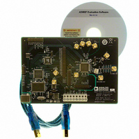
AD9957/PCBZ
Manufacturer Part Number
AD9957/PCBZ
Description
D/A Converter Evaluation Board
Manufacturer
Analog Devices Inc
Series
AgileRF™r
Datasheet
1.AD9957BSVZ-REEL.pdf
(64 pages)
Specifications of AD9957/PCBZ
Silicon Manufacturer
Analog Devices
Application Sub Type
Direct Digital Synthesizer
Kit Application Type
Clock & Timing
Silicon Core Number
AD9957
Kit Contents
Board
Main Purpose
Timing: DDS Modulators
Embedded
No
Utilized Ic / Part
AD9957
Primary Attributes
14-Bit DAC, 32-Bit Tuning Word Width
Secondary Attributes
1GHz, Graphical User Interface
Lead Free Status / RoHS Status
Lead free / RoHS Compliant
Available stocks
Company
Part Number
Manufacturer
Quantity
Price
Company:

Part Number:
AD9957/PCBZ
Manufacturer:
LT
Quantity:
962


AD9957
PLL CHARGE PUMP
The charge pump current (I
user with additional flexibility to optimize the PLL performance.
Table 8 lists the bit settings vs. the nominal charge pump
current.
Table 8. PLL Charge Pump Current
I
000
001
010
011
100
101
110
111
EXTERNAL PLL LOOP FILTER COMPONENTS
The PLL_LOOP_FILTER pin provides a connection interface to
attach the external loop filter components. The ability to use
custom loop filter components gives the user more flexibility to
optimize the PLL performance. The PLL and external loop filter
components are shown in Figure 52.
CP
(CFR3<21:19>)
PLL IN
Figure 52. REFCLK PLL External Loop Filter
REFCLK PLL
PFD
Charge Pump Current, I
212
237
262
287
312
337
363
387
CP
÷N
C1
CP
) is programmable to provide the
R1
AVDD
2
PLL_LOOP_FILTER
C2
VCO
PLL OUT
CP
(μA)
Rev. B | Page 36 of 64
In the prevailing literature, this configuration yields a third-
order, Type II PLL. To calculate the loop filter component
values, begin with the feedback divider value (N), the gain of
the phase detector (K
the programmed VCO SEL bit settings (see Table 1 for K
loop filter component values depend on the desired open-loop
bandwidth (f
where:
K
K
Ensure that proper units are used for the variables in Equation 7
through Equation 9. I
Table 8; K
loop bandwidth (f
be in radians.
For example, suppose the PLL is programmed such that
I
bandwidth and phase margin are 50 kHz and 45°, respectively,
the loop filter component values are R1 = 52.85
and C2 = 30.11 nF.
PLL LOCK INDICATION
When the PLL is in use, the PLL_LOCK pin provides an active
high indication that the PLL has locked to the REFCLK input
signal. When the PLL is bypassed, the PLL_LOCK pin defaults
to Logic 0.
CP
D
V
is taken from Table 1.
equals the programmed value of I
= 287 μA, K
C1
C2
R1
=
=
=
V
K
K
π
N
2
must be in Hz/V, not MHz/V as listed in Table 1; the
Nf
D
D
K
2 (
N
OL
K
K
D
OL
f π
) and phase margin (φ), as follows:
(
V
V
V
π
K
OL
f
= 625 MHz/V, and N = 25. If the desired loop
tan
V
OL
OL
1
)
2
) must be in Hz; the phase margin (φ) must
+
)
( )
2
D
−
φ
CP
sin
), and the gain of the VCO (K
1
must be in amps, not μA as appears in
1
cos
( )
φ
sin
( )
φ
( )
φ
CP
.
Ω, C1 = 145.4 nF,
V
) based on
V
). The
(7)
(8)
(9)
Related parts for AD9957/PCBZ
Image
Part Number
Description
Manufacturer
Datasheet
Request
R


Part Number:
Description:
±1.7g Dual-Axis IMEMS Accelerometer Evaluation Board
Manufacturer:
Analog Devices Inc
Datasheet:

Part Number:
Description:
Inertial Sensor Evaluation System
Manufacturer:
Analog Devices Inc
Datasheet:
Part Number:
Description:
Manufacturer:
Analog Devices Inc
Datasheet:
Part Number:
Description:
Manufacturer:
Analog Devices Inc
Datasheet:
Part Number:
Description:
Manufacturer:
Analog Devices Inc
Datasheet:
Part Number:
Description:
Manufacturer:
Analog Devices Inc
Datasheet:
Part Number:
Description:
Manufacturer:
Analog Devices Inc
Datasheet:
Part Number:
Description:
Manufacturer:
Analog Devices Inc
Datasheet:
Part Number:
Description:
Manufacturer:
Analog Devices Inc
Datasheet:
Part Number:
Description:
Manufacturer:
Analog Devices Inc
Datasheet:
Part Number:
Description:
Manufacturer:
Analog Devices Inc
Datasheet:
Part Number:
Description:
Manufacturer:
Analog Devices Inc
Datasheet: