AD9957/PCBZ Analog Devices Inc, AD9957/PCBZ Datasheet - Page 30
AD9957/PCBZ
Manufacturer Part Number
AD9957/PCBZ
Description
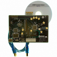
D/A Converter Evaluation Board
Manufacturer
Analog Devices Inc
Series
AgileRF™r
Datasheet
1.AD9957BSVZ-REEL.pdf
(64 pages)
Specifications of AD9957/PCBZ
Silicon Manufacturer
Analog Devices
Application Sub Type
Direct Digital Synthesizer
Kit Application Type
Clock & Timing
Silicon Core Number
AD9957
Kit Contents
Board
Main Purpose
Timing: DDS Modulators
Embedded
No
Utilized Ic / Part
AD9957
Primary Attributes
14-Bit DAC, 32-Bit Tuning Word Width
Secondary Attributes
1GHz, Graphical User Interface
Lead Free Status / RoHS Status
Lead free / RoHS Compliant
Available stocks
Company
Part Number
Manufacturer
Quantity
Price
Company:

Part Number:
AD9957/PCBZ
Manufacturer:
LT
Quantity:
962


AD9957
RAM Bidirectional Ramp Mode
This mode is unique in that the RAM segment playback mode
word of both RAM segment registers must be programmed for
RAM bidirectional ramp mode.
In bidirectional ramp mode, upon assertion of an I/O update,
the RAM readies for playback operation using the parameters
programmed into RAM Segment Register 0. The data is deliv-
ered at the appropriate rate and to the destination as specified
by the RAM playback destination bit.
The playback rate is governed by the timer that is internal to the
RAM state machine, and its period (Δt) is determined by the
state of the RAM playback destination bit as detailed in the
RAM Playback Operation section.
Playback begins upon a 0 to 1 logic transition on the RT pin.
This instructs the state machine to increment through the
address range specified in RAM Segment Register 0 starting
with the start address. As long as the RT pin remains Logic 1,
the state machine continues to play back the RAM data until it
reaches the end address, at which point the state machine halts.
I/O_UPDATE
ADDRESS
ADDRESS
RAM
RAM
PIN
RAM SEGMENT
RT
1
M DDS CLOCK CYCLES
1 PDCLK CYCLE
2
OR
END ADDRESS
NUMBER 0
START ADDRESS NUMBER 0
END ADDRESS NUMBER 1
START ADDRESS NUMBER 1
0
1
Δ
t
Figure 44. Bidirectional Ramp Timing Diagram
3
Rev. B | Page 30 of 64
4
1
Δ
t
A Logic 1 to Logic 0 transition on the RT pin instructs the state
machine to switch to RAM Segment Register 1 and to decrement
through the address range starting with the end address. As
long as the RT pin remains Logic 0, the state machine continues
to play back the RAM data until it reaches the start address, at
which point the state machine halts.
It is important to note that RAM Segment Register 1 is played
back in reverse order for bidirectional ramp mode. This must
be kept in mind when the RAM contents are loaded via the
serial I/O port when bidirectional ramp mode is the intended
playback mode.
A graphic representation of the bidirectional ramp mode
appears in Figure 44. It demonstrates the action of the state
machine in response to the RT pin. If the RT pin changes states
before the state machine reaches the programmed start or end
address, the internal timer is restarted and the direction of the
address counter reversed.
5
Δ
0
t
6
Δ
t
1
7
8
0
Δ
t
Related parts for AD9957/PCBZ
Image
Part Number
Description
Manufacturer
Datasheet
Request
R


Part Number:
Description:
±1.7g Dual-Axis IMEMS Accelerometer Evaluation Board
Manufacturer:
Analog Devices Inc
Datasheet:

Part Number:
Description:
Inertial Sensor Evaluation System
Manufacturer:
Analog Devices Inc
Datasheet:
Part Number:
Description:
Manufacturer:
Analog Devices Inc
Datasheet:
Part Number:
Description:
Manufacturer:
Analog Devices Inc
Datasheet:
Part Number:
Description:
Manufacturer:
Analog Devices Inc
Datasheet:
Part Number:
Description:
Manufacturer:
Analog Devices Inc
Datasheet:
Part Number:
Description:
Manufacturer:
Analog Devices Inc
Datasheet:
Part Number:
Description:
Manufacturer:
Analog Devices Inc
Datasheet:
Part Number:
Description:
Manufacturer:
Analog Devices Inc
Datasheet:
Part Number:
Description:
Manufacturer:
Analog Devices Inc
Datasheet:
Part Number:
Description:
Manufacturer:
Analog Devices Inc
Datasheet:
Part Number:
Description:
Manufacturer:
Analog Devices Inc
Datasheet: