AD9957/PCBZ Analog Devices Inc, AD9957/PCBZ Datasheet - Page 60
AD9957/PCBZ
Manufacturer Part Number
AD9957/PCBZ
Description
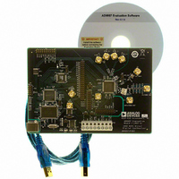
D/A Converter Evaluation Board
Manufacturer
Analog Devices Inc
Series
AgileRF™r
Datasheet
1.AD9957BSVZ-REEL.pdf
(64 pages)
Specifications of AD9957/PCBZ
Silicon Manufacturer
Analog Devices
Application Sub Type
Direct Digital Synthesizer
Kit Application Type
Clock & Timing
Silicon Core Number
AD9957
Kit Contents
Board
Main Purpose
Timing: DDS Modulators
Embedded
No
Utilized Ic / Part
AD9957
Primary Attributes
14-Bit DAC, 32-Bit Tuning Word Width
Secondary Attributes
1GHz, Graphical User Interface
Lead Free Status / RoHS Status
Lead free / RoHS Compliant
Available stocks
Company
Part Number
Manufacturer
Quantity
Price
Company:

Part Number:
AD9957/PCBZ
Manufacturer:
LT
Quantity:
962


AD9957
PROFILE REGISTERS
There are eight consecutive serial I/O addresses (0x0E to 0x15)
dedicated to device profiles. All eight profile registers are either
single tone profiles or QDUC profiles depending on the device
operating mode specified by CFR1<25:24>. During operation,
the active profile register is determined via the external
PROFILE<2:0> pins.
Single tone profiles control: DDS frequency (32 bits), DDS
phase offset (16 bits), and DDS amplitude scaling (14 bits).
Profile<7:0> Register—Single Tone
Address 0x0E to 0x15, eight bytes are assigned to this register.
Table 27. Bit Descriptions for Profile<7:0> Registers—Single Tone
Bit(s)
63:62
61:48
47:32
31:0
Profile<7:0> Register—QDUC
Address 0x0E to 0x15, eight bytes are assigned to this register.
Table 28. Bit Descriptions for Profile<7:0> Registers—QDUC
Bit(s)
63:58
57
56
55:48
47:32
31:0
RAM Register
Address 0x16, four bytes are assigned to this register.
Table 29. Bit Descriptions for RAM Register
Bit(s)
31:0
GPIO Configuration Register
Address 0x18, two bytes are assigned to this register.
Table 30. Bit Descriptions for GPIO Configuration Register
Bit(s)
15:0
GPIO Data Register
Address 0x19, two bytes are assigned to this register.
Table 31. Bit Descriptions for GPIO Data Register
Bits
15:0
Mnemonic
CC Interpolation Rate
Spectral Invert
Inverse CCI Bypass
Output Scale Factor
Phase Offset Word
Frequency Tuning Word
Mnemonic
RAM Word
Mnemonic
GPIO Configuration
Mnemonic
Open
Amplitude Scale Factor
Phase Offset Word
Frequency Tuning Word
Mnemonic
GPIO Data
Description
Read or write based on the contents of the GPIO Configuration register. See the
General-Purpose I/O (GPIO) Port section for details.
Description
This 14-bit number controls the DDS output amplitude.
This 16-bit number controls the DDS phase offset.
This 32-bit number controls the DDS frequency.
Description
This 6-bit number is the rate interpolation factor for the CCI filter.
0: the modulator output takes the form: I(t) × cos(ct) – Q(t) × sin(ct).
1: the modulator output takes the form: I(t) × cos(ct) + Q(t) × sin(ct).
0: the inverse CCI filter is enabled.
1: the inverse CCI filter is bypassed.
This 8-bit number controls the output amplitude.
This 16-bit number controls the DDS phase offset.
This 32-bit number controls the DDS frequency.
Description
The number of 32-bit words written to RAM is defined by the start and end address in
RAM Segment Register 0 or RAM Segment Register 1.
Description
See the General-Purpose I/O (GPIO) Port section for details.
Rev. B | Page 60 of 64
QDUC profiles control: DDS frequency (32 bits), DDS phase
offset (16 bits), output amplitude scaling (8 bits), CCI filter
interpolation factor, inverse CCI bypass, and spectral invert.
The QDUC profiles also selectively apply to the interpolating
DAC operating mode: only output scaling, CCI filter interpola-
tion factor, and inverse CCI bypass apply; all others (DDS
frequency, output amplitude scaling, and spectral invert) are
ignored.
Related parts for AD9957/PCBZ
Image
Part Number
Description
Manufacturer
Datasheet
Request
R


Part Number:
Description:
±1.7g Dual-Axis IMEMS Accelerometer Evaluation Board
Manufacturer:
Analog Devices Inc
Datasheet:

Part Number:
Description:
Inertial Sensor Evaluation System
Manufacturer:
Analog Devices Inc
Datasheet:
Part Number:
Description:
Manufacturer:
Analog Devices Inc
Datasheet:
Part Number:
Description:
Manufacturer:
Analog Devices Inc
Datasheet:
Part Number:
Description:
Manufacturer:
Analog Devices Inc
Datasheet:
Part Number:
Description:
Manufacturer:
Analog Devices Inc
Datasheet:
Part Number:
Description:
Manufacturer:
Analog Devices Inc
Datasheet:
Part Number:
Description:
Manufacturer:
Analog Devices Inc
Datasheet:
Part Number:
Description:
Manufacturer:
Analog Devices Inc
Datasheet:
Part Number:
Description:
Manufacturer:
Analog Devices Inc
Datasheet:
Part Number:
Description:
Manufacturer:
Analog Devices Inc
Datasheet:
Part Number:
Description:
Manufacturer:
Analog Devices Inc
Datasheet: