AD9957/PCBZ Analog Devices Inc, AD9957/PCBZ Datasheet - Page 49
AD9957/PCBZ
Manufacturer Part Number
AD9957/PCBZ
Description
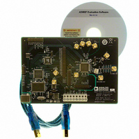
D/A Converter Evaluation Board
Manufacturer
Analog Devices Inc
Series
AgileRF™r
Datasheet
1.AD9957BSVZ-REEL.pdf
(64 pages)
Specifications of AD9957/PCBZ
Silicon Manufacturer
Analog Devices
Application Sub Type
Direct Digital Synthesizer
Kit Application Type
Clock & Timing
Silicon Core Number
AD9957
Kit Contents
Board
Main Purpose
Timing: DDS Modulators
Embedded
No
Utilized Ic / Part
AD9957
Primary Attributes
14-Bit DAC, 32-Bit Tuning Word Width
Secondary Attributes
1GHz, Graphical User Interface
Lead Free Status / RoHS Status
Lead free / RoHS Compliant
Available stocks
Company
Part Number
Manufacturer
Quantity
Price
Company:

Part Number:
AD9957/PCBZ
Manufacturer:
LT
Quantity:
962


I/O_UPDATE, SYNC_CLK, AND SYSTEM CLOCK
RELATIONSHIPS
The I/O_UPDATE pin is used to transfer data from the serial
I/O buffer to the active registers in the device. Data in the buffer
is inactive.
SYNC_CLK is a rising edge active signal. It is derived from the
system clock and a divide-by-4 frequency divider. SYNC_CLK,
which is externally provided, can be used to synchronize
external hardware to the AD9957 internal clocks.
I/O_UPDATE initiates the start of a buffer transfer. It can
be sent synchronously or asynchronously relative to the
SYNC_CLK. If the setup time between these signals is met,
then constant latency (pipeline) to the DAC output exists.
I/O BUFFERS
THE DEVICE REGISTERS AN I/O UPDATE AT POINT A. THE DATA IS TRANSFERRED FROM THE ASYNCHRONOUSLY LOADED I/O BUFFERS AT POINT B.
I/O_UPDATE
REGISTERS
SYNC_CLK
DATA IN
SYSCLK
DATA IN
N
N – 1
Figure 64. I/O_UPDATE Transferring Data from I/O Buffer to Active Registers
A
B
N + 1
Rev. B | Page 49 of 64
For example, if repetitive changes to phase offset via the SPI
port is desired, the latency of those changes to the DAC output
is constant; otherwise, a time uncertainty of one SYNC_CLK
period is present.
By default, the I/O_UPDATE pin is an input that serves as a
strobe signal to allow synchronous update of the device oper-
ating parameters. A rising edge on I/O_UPDATE initiates
transfer of the register contents to the internal workings of
the device. Alternatively, the transfer of programmed data from
the programming registers to the internal hardware can be
accomplished by changing the state of the PROFILE[2:0] pins.
The timing diagram shown in Figure 64 depicts when the data
in the buffer is transferred to the active registers.
N
N + 2
N + 1
AD9957
Related parts for AD9957/PCBZ
Image
Part Number
Description
Manufacturer
Datasheet
Request
R


Part Number:
Description:
±1.7g Dual-Axis IMEMS Accelerometer Evaluation Board
Manufacturer:
Analog Devices Inc
Datasheet:

Part Number:
Description:
Inertial Sensor Evaluation System
Manufacturer:
Analog Devices Inc
Datasheet:
Part Number:
Description:
Manufacturer:
Analog Devices Inc
Datasheet:
Part Number:
Description:
Manufacturer:
Analog Devices Inc
Datasheet:
Part Number:
Description:
Manufacturer:
Analog Devices Inc
Datasheet:
Part Number:
Description:
Manufacturer:
Analog Devices Inc
Datasheet:
Part Number:
Description:
Manufacturer:
Analog Devices Inc
Datasheet:
Part Number:
Description:
Manufacturer:
Analog Devices Inc
Datasheet:
Part Number:
Description:
Manufacturer:
Analog Devices Inc
Datasheet:
Part Number:
Description:
Manufacturer:
Analog Devices Inc
Datasheet:
Part Number:
Description:
Manufacturer:
Analog Devices Inc
Datasheet:
Part Number:
Description:
Manufacturer:
Analog Devices Inc
Datasheet: