AD9957/PCBZ Analog Devices Inc, AD9957/PCBZ Datasheet - Page 58
AD9957/PCBZ
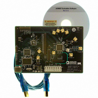
Manufacturer Part Number
AD9957/PCBZ
Description
D/A Converter Evaluation Board
Manufacturer
Analog Devices Inc
Series
AgileRF™r
Datasheet
1.AD9957BSVZ-REEL.pdf
(64 pages)
Specifications of AD9957/PCBZ
Silicon Manufacturer
Analog Devices
Application Sub Type
Direct Digital Synthesizer
Kit Application Type
Clock & Timing
Silicon Core Number
AD9957
Kit Contents
Board
Main Purpose
Timing: DDS Modulators
Embedded
No
Utilized Ic / Part
AD9957
Primary Attributes
14-Bit DAC, 32-Bit Tuning Word Width
Secondary Attributes
1GHz, Graphical User Interface
Lead Free Status / RoHS Status
Lead free / RoHS Compliant
Available stocks
Company
Part Number
Manufacturer
Quantity
Price
Company:

Part Number:
AD9957/PCBZ
Manufacturer:
LT
Quantity:
962


AD9957
Control Function Register 3 (CFR3)
Address 0x02, four bytes are assigned to this register.
Table 20. Bit Descriptions for CFR3 Register
Bit (s)
31:30
29:28
27
26:24
23:22
21:19
18:16
15
14
13:9
8
7:1
0
Auxiliary DAC Control Register
Address 0x03, four bytes are assigned to this register.
Table 21. Bit Descriptions for Auxiliary DAC Control Register
Bit(s)
31:8
7:0
I/O Update Rate Register
Address 0x04, four bytes are assigned to this register. This register is effective without the need for an I/O update.
Table 22. Bit Descriptions for I/O Update Rate Register5
Bit(s)
31:0
RAM Segment Register 0
Address 0x05, six bytes are assigned to this register. This register is effective without the need for an I/O update. This register is only
active if CFR1<31> = 1 and there is a Logic 0-to-Logic 1 transition on the RT pin.
Table 23. Bit Descriptions for RAM Segment Register 0
Bit(s)
47:32
31:22
21:16
15:6
5:3
2:0
Mnemonic
I/O Update Rate
Mnemonic
Open
FSC
Mnemonic
RAM Address Step
Rate 0
RAM End Address 0
Open
RAM Start Address 0
Open
RAM Playback Mode 0
Mnemonic
Open
DRV0
Open
VCO SEL
Open
I
Open
REFCLK Input Divider
Bypass
REFCLK Input Divider
ResetB
Open
PLL Enable
N
Open
CP
Description
Controls REFCLK_OUT pin (see Table 6 for details); default is 01b.
Selects frequency band of the VCO in the REFCLK PLL (see Table 7 for details); default is 111b.
Selects the charge pump current in the REFCLK PLL (see Table 8 for details); default is 111b.
0: input divider is selected (default).
1: input divider is bypassed.
0: input divider is reset.
1: input divider operates normally (default).
0: REFCLK PLL bypassed (default).
1: REFCLK PLL enabled.
This 7-bit number is divide modulus of the REFCLK PLL feedback divider; default is 0000000b.
Description
This 8-bit number controls the full-scale output current of the main DAC (see the Auxiliary DAC section);
default is 0xFF.
Description
This 16-bit number controls the rate at which the RAM state machine steps through the specified RAM
address range.
This 10-bit number identifies the ending address for the RAM state machine.
This 10-bit number identifies the starting address for the RAM state machine.
This 3-bit number identifies the playback mode for the RAM state machine (see Table 5).
Description
Ineffective unless CFR2<23> = 1. This 32-bit number controls the automatic I/O update rate (see the
Automatic I/O Update section); default is 0xFFFFFFFF.
Rev. B | Page 58 of 64
Related parts for AD9957/PCBZ
Image
Part Number
Description
Manufacturer
Datasheet
Request
R


Part Number:
Description:
±1.7g Dual-Axis IMEMS Accelerometer Evaluation Board
Manufacturer:
Analog Devices Inc
Datasheet:

Part Number:
Description:
Inertial Sensor Evaluation System
Manufacturer:
Analog Devices Inc
Datasheet:
Part Number:
Description:
Manufacturer:
Analog Devices Inc
Datasheet:
Part Number:
Description:
Manufacturer:
Analog Devices Inc
Datasheet:
Part Number:
Description:
Manufacturer:
Analog Devices Inc
Datasheet:
Part Number:
Description:
Manufacturer:
Analog Devices Inc
Datasheet:
Part Number:
Description:
Manufacturer:
Analog Devices Inc
Datasheet:
Part Number:
Description:
Manufacturer:
Analog Devices Inc
Datasheet:
Part Number:
Description:
Manufacturer:
Analog Devices Inc
Datasheet:
Part Number:
Description:
Manufacturer:
Analog Devices Inc
Datasheet:
Part Number:
Description:
Manufacturer:
Analog Devices Inc
Datasheet:
Part Number:
Description:
Manufacturer:
Analog Devices Inc
Datasheet: