AD9957/PCBZ Analog Devices Inc, AD9957/PCBZ Datasheet - Page 11
AD9957/PCBZ
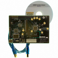
Manufacturer Part Number
AD9957/PCBZ
Description
D/A Converter Evaluation Board
Manufacturer
Analog Devices Inc
Series
AgileRF™r
Datasheet
1.AD9957BSVZ-REEL.pdf
(64 pages)
Specifications of AD9957/PCBZ
Silicon Manufacturer
Analog Devices
Application Sub Type
Direct Digital Synthesizer
Kit Application Type
Clock & Timing
Silicon Core Number
AD9957
Kit Contents
Board
Main Purpose
Timing: DDS Modulators
Embedded
No
Utilized Ic / Part
AD9957
Primary Attributes
14-Bit DAC, 32-Bit Tuning Word Width
Secondary Attributes
1GHz, Graphical User Interface
Lead Free Status / RoHS Status
Lead free / RoHS Compliant
Available stocks
Company
Part Number
Manufacturer
Quantity
Price
Company:

Part Number:
AD9957/PCBZ
Manufacturer:
LT
Quantity:
962


Pin No.
59
60
67
68
69
70
71
80
81
84
90
91
94
95
96 (EPAD)
1
I = input, O = output.
Mnemonic
I/O_UPDATE
OSK
SDIO
SDO
SCLK
CS
I/O_RESET
IOUT
IOUT
DAC_RSET
REF_CLK
REF_CLK
REFCLK_OUT
XTAL_SEL
Exposed Pad
(EPAD)
I/O
I/O
I
I/O
O
I
I
I
O
O
O
I
I
O
I
1
Description
Input/Output Update; Digital Input Or Output (Active High) Depending on the Internal I/O
Update Active Bit. A high on this pin indicates a transfer of the contents of the I/O buffers
to the corresponding internal registers.
Output Shift Keying, Digital Input (Active High). When using OSK (manual or automatic),
this pin controls the OSK function. See the Output Shift Keying (OSK) section of the data
sheet for details. When not using OSK, tie this pin high.
Serial Data Input/Output, Digital Input/Output (Active High). This pin can be either
unidirectional or bidirectional (default), depending on configuration settings. In
bidirectional serial port mode, this pin acts as the serial data input and output. In
unidirectional, it is an input only.
Serial Data Output, Digital Output (Active High). This pin is only active in unidirectional
serial data mode. In this mode, it functions as the output. In bidirectional mode, this pin is
not operational and should be left floating.
Serial Data Clock. Digital clock (rising edge on write, falling edge on read). This pin
provides the serial data clock for the control data path. Write operations to the AD9957
use the rising edge. Readback operations from the AD9957 use the falling edge.
Chip Select, Digital Input (Active Low). Bringing this pin low enables the AD9957 to detect
serial clock rising/falling edges. Bringing this pin high causes the AD9957 to ignore input
on the serial data pins.
Input/Output Reset, Digital Input (Active High). Rather than resetting the entire device
during a failed communication cycle, when brought high, this pin resets the state machine
of the serial port controller and clears any I/O buffers that have been written since the last
I/O update. When unused, tie this pin to ground to avoid accidental resets.
Open-Source DAC Complementary Output Source. Analog output, current mode. Connect
through 50 Ω to AGND.
Open-Source DAC Output Source. Analog output, current mode. Connect through 50 Ω to
AGND.
Analog Reference Pin. This pin programs the DAC output full-scale reference current.
Attach a 10 kΩ resistor to AGND.
Reference Clock Input. Analog input. See the REFCLK Overview section for more details.
Complementary Reference Clock Input. Analog input. See the REFCLK Overview section
for more details.
Reference Clock Output. Analog output. See the REFCLK Overview section for more
details.
Crystal Select (1.8 V Logic). Analog input (active high). Driving the XTAL_SEL pin high enables
the internal oscillator to be used with a crystal resonator. If unused, connect it to AGND.
The EPAD should be soldered to ground.
Rev. B | Page 11 of 64
AD9957
Related parts for AD9957/PCBZ
Image
Part Number
Description
Manufacturer
Datasheet
Request
R


Part Number:
Description:
±1.7g Dual-Axis IMEMS Accelerometer Evaluation Board
Manufacturer:
Analog Devices Inc
Datasheet:

Part Number:
Description:
Inertial Sensor Evaluation System
Manufacturer:
Analog Devices Inc
Datasheet:
Part Number:
Description:
Manufacturer:
Analog Devices Inc
Datasheet:
Part Number:
Description:
Manufacturer:
Analog Devices Inc
Datasheet:
Part Number:
Description:
Manufacturer:
Analog Devices Inc
Datasheet:
Part Number:
Description:
Manufacturer:
Analog Devices Inc
Datasheet:
Part Number:
Description:
Manufacturer:
Analog Devices Inc
Datasheet:
Part Number:
Description:
Manufacturer:
Analog Devices Inc
Datasheet:
Part Number:
Description:
Manufacturer:
Analog Devices Inc
Datasheet:
Part Number:
Description:
Manufacturer:
Analog Devices Inc
Datasheet:
Part Number:
Description:
Manufacturer:
Analog Devices Inc
Datasheet:
Part Number:
Description:
Manufacturer:
Analog Devices Inc
Datasheet: