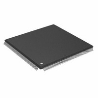
ADSP-21065LCSZ-240 Analog Devices Inc, ADSP-21065LCSZ-240 Datasheet - Page 20

ADSP-21065LCSZ-240
Manufacturer Part Number
ADSP-21065LCSZ-240
Description
ADSP-21065L 60 Mhz
Manufacturer
Analog Devices Inc
Series
SHARC®r
Type
Fixed/Floating Pointr
Datasheet
1.ADSP-21065LKSZ-240.pdf
(44 pages)
Specifications of ADSP-21065LCSZ-240
Interface
Host Interface, Serial Port
Clock Rate
60MHz
Non-volatile Memory
External
On-chip Ram
64kB
Voltage - I/o
3.30V
Voltage - Core
3.30V
Operating Temperature
-40°C ~ 100°C
Mounting Type
Surface Mount
Package / Case
208-MQFP, 208-PQFP
Device Core Size
32b
Architecture
Enhanced Harvard
Format
Floating Point
Clock Freq (max)
60MHz
Mips
60
Device Input Clock Speed
60MHz
Ram Size
68KB
Operating Supply Voltage (typ)
3.3V
Operating Supply Voltage (min)
3.13V
Operating Supply Voltage (max)
3.6V
Operating Temp Range
-40C to 100C
Operating Temperature Classification
Industrial
Mounting
Surface Mount
Pin Count
208
Package Type
MQFP
Lead Free Status / RoHS Status
Lead free / RoHS Compliant
Lead Free Status / RoHS Status
Lead free / RoHS Compliant
Other names
ADS-P21065LCSZ240
ADS-P21065LCSZ240
ADS-P21065LCSZ240
Available stocks
Company
Part Number
Manufacturer
Quantity
Price
Company:
Part Number:
ADSP-21065LCSZ-240
Manufacturer:
AD
Quantity:
310
Company:
Part Number:
ADSP-21065LCSZ-240
Manufacturer:
Analog Devices Inc
Quantity:
10 000
ADSP-21065L
Synchronous Read/Write—Bus Slave
Use these specifications for ADSP-21065L bus master accesses of a slave’s IOP registers or internal memory (in multiprocessor
memory space). The bus master must meet these (bus slave) timing requirements.
Parameter
Timing Requirements:
t
t
t
t
t
t
t
Switching Characteristics:
t
t
t
t
NOTES
1
2
For two ADSP-21065Ls to communicate synchronously as master and slave, certain master and slave specification combinations
must be satisfied. Do not compare specification values directly to calculate master/slave clock skew margins for those specifications
listed below. The following table shows the appropriate clock skew margin.
t
See System Hold Time Calculation under Test Conditions for calculation of hold times given capacitive and dc loads.
SADRI
HADRI
SRWLI
HRWLI
RWHPI
SDATWH
HDATWH
SDDATO
DATTR
DACK
ACKTR
SRWLI
is specified when Multiprocessor Memory Space Wait State (MMSWS bit in WAIT register) is disabled; when MMSWS is enabled, t
Address, SW Setup Before CLKIN
Address, SW Hold Before CLKIN
RD/WR Low Setup Before CLKIN
RD/WR Low Hold After CLKIN
RD/WR Pulse High
Data Setup Before WR High
Data Hold After WR High
Data Delay After CLKIN
Data Disable After CLKIN
ACK Delay After CLKIN
ACK Disable After CLKIN
Master Specification
t
t
t
t
t
t
SSDATI
SACKC
DADRO
DRWL
DRDO
DWRO
(Max)
(Max)
(Max)
2
2
Table IV. Bus Master to Slave Skew Margins
1
Slave Specification
t
t
t
t
t
t
SDDATO
DACK
SADRI
SRWLI
HRWLI
HRWLI
(Max)
(Max)
–20–
Skew Margin
t
t
t
t
t
t
t
t
t
t
t
t
CK
CK
CK
CK
CK
CK
CK
CK
CK
CK
CK
CK
Min
24.5 + 25 DT
21.0 + 21 DT
2.5
4.5
0.0
1.0 – 2 DT
1.0 – 2 DT
–2.50 – 5 DT
= 33.3 ns
= 30.0 ns
= 33.3 ns
= 30.0 ns
= 33.3 ns
= 30.0 ns
= 33.3 ns
= 30.0 ns
= 33.3 ns
= 30.0 ns
= 33.3 ns
= 30.0 ns
+ 1.50 ns
+ 3.00 ns
+ 2.25 ns
N/A
+ 2.75 ns
+ 1.50 ns
+ 1.25 ns
N/A
3.00 ns
N/A
3.75 ns
+ 2.25 ns
Max
4.0 + 8 DT
7.5 + 7 DT
31.75 + 21 DT
7.0 – 2 DT
29.5 + 20 DT
6.0 – 2 DT
SRWLI
(min) = 17.5 + 18 DT.
REV. C
Unit
ns
ns
ns
ns
ns
ns
ns
ns
ns
ns
ns


